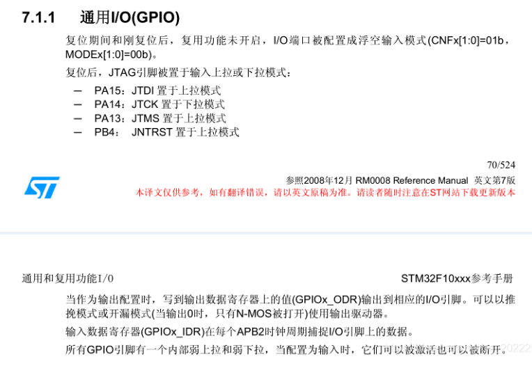
STM32单片机复位后,JTAG口默认是被占用的。如果想将JTAG占用的几个IO口设置为普通IO口,就需要进行端口重映射。1 x$ G0 L1 A9 M" B' E1 _5 \
5 R7 p1 H$ k4 U* D" O4 Y
复位后端口默认功能可以在STM32参考手册上看到0 J! z+ Y8 ^* @6 w8 y6 p
$ p1 D& @% S. M+ q; s6 g
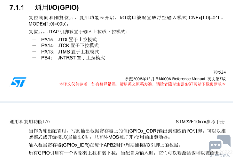
) `; ]( ] L. M- c: g) c5 R- Z+ t1 O0 q( h y- R T' a/ e3 i
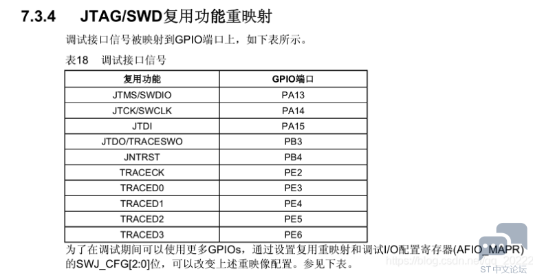
要将JTAG占用的这些口设置为普通IO口时,需要用复用功能重映射,在程序开始执行时将JTAG口重映射为普通IO口。
/ l/ _. q `1 D% h
7 O& |3 d* j0 }
 4 `5 k- a8 n w! P; F/ ?7 n8 Y( q
![EOVLF[$T~GV[5$@CAT`_@R1.png](data/attachment/forum/202203/21/131211b2zee8008es82xkk.png "EOVLF[$T~GV[5$@CAT`_@R1.png") 9 T d# X) F5 L' Q8 J. \; s) d
+ T: o: [( y( r4 m将JTAG要设置为普通 IO口时,需要设置AFIO_MAPR寄存器的SWJ_CFG位。如果用寄存器操作的话,就直接设置这个寄存器的值就行。如果用库函数操作的话,可以直接调用库函数void GPIO_PinRemapConfig(uint32_t GPIO_Remap, FunctionalState NewState)。8 N3 U" G: O6 x$ ]
! o1 R" J9 p" ]: {
这个库函数的具体实现可以在stm32f10x_gpio.c这个文件中查看,具体代码如下:
6 b* T9 c9 R( ]& i- q
4 M& C4 \8 m" s! z3 d2 ?- /**
0 w/ J# Z3 |# Z P - * @brief Changes the mapping of the specified pin.2 J m' V: j; Y
- * @param GPIO_Remap: selects the pin to remap.$ Y- t! k' `& n- v& ~
- * This parameter can be one of the following values:
$ Z# P- R8 n$ `/ p# D - * @arg GPIO_Remap_SPI1 : SPI1 Alternate Function mapping
& \) V& C d" D8 l. X& m: V* C - * @arg GPIO_Remap_I2C1 : I2C1 Alternate Function mapping, E# V8 Y$ n0 t' h' f
- * @arg GPIO_Remap_USART1 : USART1 Alternate Function mapping. u: w8 }- H% b. i" v
- * @arg GPIO_Remap_USART2 : USART2 Alternate Function mapping) k' r; I7 m; j
- * @arg GPIO_PartialRemap_USART3 : USART3 Partial Alternate Function mapping; w& L$ D/ Q' P0 w% k7 f7 U
- * @arg GPIO_FullRemap_USART3 : USART3 Full Alternate Function mapping8 f- E }7 b3 E9 U) v
- * @arg GPIO_PartialRemap_TIM1 : TIM1 Partial Alternate Function mapping
# y. Q+ L; h, e% ^0 \- q9 R - * @arg GPIO_FullRemap_TIM1 : TIM1 Full Alternate Function mapping
, b) Q. h2 L$ Q6 ] - * @arg GPIO_PartialRemap1_TIM2 : TIM2 Partial1 Alternate Function mapping
) g2 z: B& ]" m - * @arg GPIO_PartialRemap2_TIM2 : TIM2 Partial2 Alternate Function mapping8 y$ j2 l* J* V( T! z8 B
- * @arg GPIO_FullRemap_TIM2 : TIM2 Full Alternate Function mapping, E& l m% Z+ e
- * @arg GPIO_PartialRemap_TIM3 : TIM3 Partial Alternate Function mapping
$ s6 e- i K/ H% Q5 _ - * @arg GPIO_FullRemap_TIM3 : TIM3 Full Alternate Function mapping
' q7 X7 c% X# R! u5 B* P - * @arg GPIO_Remap_TIM4 : TIM4 Alternate Function mapping( @; P, p; d: u
- * @arg GPIO_Remap1_CAN1 : CAN1 Alternate Function mapping! r* J4 n7 e$ i8 s* _* i
- * @arg GPIO_Remap2_CAN1 : CAN1 Alternate Function mapping
' q' R7 ~ Y1 q) |/ }0 M - * @arg GPIO_Remap_PD01 : PD01 Alternate Function mapping) \! ~! |; z2 G* [* z
- * @arg GPIO_Remap_TIM5CH4_LSI : LSI connected to TIM5 Channel4 input capture for calibration& s) Z! p% ~/ \: d
- * @arg GPIO_Remap_ADC1_ETRGINJ : ADC1 External Trigger Injected Conversion remapping
D* M; n6 E5 Z* E- S - * @arg GPIO_Remap_ADC1_ETRGREG : ADC1 External Trigger Regular Conversion remapping+ i5 Q4 j. {0 J; O! W( p) C
- * @arg GPIO_Remap_ADC2_ETRGINJ : ADC2 External Trigger Injected Conversion remapping
$ m8 m9 U) `" y% f+ b( H - * @arg GPIO_Remap_ADC2_ETRGREG : ADC2 External Trigger Regular Conversion remapping
: \# X/ R9 Q! ~# ]" e - * @arg GPIO_Remap_ETH : Ethernet remapping (only for Connectivity line devices)
- R' b7 y% j2 y, h& u, l, M" e$ E - * @arg GPIO_Remap_CAN2 : CAN2 remapping (only for Connectivity line devices)( D4 T, R+ ~ t7 a9 \- J# V4 E
- * @arg GPIO_Remap_SWJ_NoJTRST : Full SWJ Enabled (JTAG-DP + SW-DP) but without JTRST3 f- f+ m; m# {% h( j: x" M
- * @arg GPIO_Remap_SWJ_JTAGDisable : JTAG-DP Disabled and SW-DP Enabled/ T* Y1 j/ V! a" A. j$ p* P% j5 p" V
- * @arg GPIO_Remap_SWJ_Disable : Full SWJ Disabled (JTAG-DP + SW-DP)
* N. L7 _$ ~" A - * @arg GPIO_Remap_SPI3 : SPI3/I2S3 Alternate Function mapping (only for Connectivity line devices)1 I8 v4 n: ~9 D8 }+ J( ]/ R) w
- * When the SPI3/I2S3 is remapped using this function, the SWJ is configured
! X$ U, K# Z% ^& x3 l# a; g - * to Full SWJ Enabled (JTAG-DP + SW-DP) but without JTRST. 2 x; _! M. a4 p# k
- * @arg GPIO_Remap_TIM2ITR1_PTP_SOF : Ethernet PTP output or USB OTG SOF (Start of Frame) connected" L' B* P" d; u+ l
- * to TIM2 Internal Trigger 1 for calibration (only for Connectivity line devices)
# q6 X: o' D5 o6 j5 m W' H) t2 ? - * If the GPIO_Remap_TIM2ITR1_PTP_SOF is enabled the TIM2 ITR1 is connected to 3 m: Q& K+ f. G+ \2 l7 N6 h
- * Ethernet PTP output. When Reset TIM2 ITR1 is connected to USB OTG SOF output. ) r0 @ U( r& b2 S5 ]0 `+ ~
- * @arg GPIO_Remap_PTP_PPS : Ethernet MAC PPS_PTS output on PB05 (only for Connectivity line devices)
2 h( K4 _; x/ r2 S7 f2 B2 Z - * @arg GPIO_Remap_TIM15 : TIM15 Alternate Function mapping (only for Value line devices)
2 v e( j. W! B9 B - * @arg GPIO_Remap_TIM16 : TIM16 Alternate Function mapping (only for Value line devices)" f$ C! ?/ x" ]# e) d9 E
- * @arg GPIO_Remap_TIM17 : TIM17 Alternate Function mapping (only for Value line devices)- @! g% A7 y. g6 P' z- `+ h2 F
- * @arg GPIO_Remap_CEC : CEC Alternate Function mapping (only for Value line devices)
! Z% s6 I0 |7 Z1 f" ~( k0 g' o( n - * @arg GPIO_Remap_TIM1_DMA : TIM1 DMA requests mapping (only for Value line devices)
, D7 C7 `9 }% d5 R5 e, P - * @arg GPIO_Remap_TIM9 : TIM9 Alternate Function mapping (only for XL-density devices)
: Q7 i$ m, y8 }; S$ w' y - * @arg GPIO_Remap_TIM10 : TIM10 Alternate Function mapping (only for XL-density devices)1 O! l' Q" a8 T" s% Z9 l
- * @arg GPIO_Remap_TIM11 : TIM11 Alternate Function mapping (only for XL-density devices)( R1 t+ Z/ t% l7 r6 o' c' l, @3 _- ?
- * @arg GPIO_Remap_TIM13 : TIM13 Alternate Function mapping (only for High density Value line and XL-density devices) z1 s# r4 i( B! P5 m# z
- * @arg GPIO_Remap_TIM14 : TIM14 Alternate Function mapping (only for High density Value line and XL-density devices)
* B& y3 g% P5 E% L$ d5 { - * @arg GPIO_Remap_FSMC_NADV : FSMC_NADV Alternate Function mapping (only for High density Value line and XL-density devices)3 {9 I; U' k( I/ q2 r: X, F" U
- * @arg GPIO_Remap_TIM67_DAC_DMA : TIM6/TIM7 and DAC DMA requests remapping (only for High density Value line devices)
3 l: S3 R; F9 k3 i, \/ q0 _ - * @arg GPIO_Remap_TIM12 : TIM12 Alternate Function mapping (only for High density Value line devices)
* B6 H7 s2 c& g. G6 [6 F1 x - * @arg GPIO_Remap_MISC : Miscellaneous Remap (DMA2 Channel5 Position and DAC Trigger remapping, & |* Q& A5 U& _5 }2 t
- * only for High density Value line devices) $ U' g h: ?( [1 X
- * @param NewState: new state of the port pin remapping.
0 d- b6 F( r* H, S" N) L - * This parameter can be: ENABLE or DISABLE.
7 m0 c) Z7 v& w5 r - * @retval None7 r, l, X% D: H* E! q% u7 r: n
- */8 J3 [+ `/ j" k8 N& K8 ?5 }" Q* P
- void GPIO_PinRemapConfig(uint32_t GPIO_Remap, FunctionalState NewState)
5 O" c$ N6 i/ ^3 I X6 o9 t - {
( z- M) n( ~/ {5 z2 v - uint32_t tmp = 0x00, tmp1 = 0x00, tmpreg = 0x00, tmpmask = 0x00;
, g$ A: x; }; A4 g7 s% q# l* @ - 8 G5 [5 v8 Z* {" c- l: J
- /* Check the parameters */
1 ?) ^. j! L: t1 @* | - assert_param(IS_GPIO_REMAP(GPIO_Remap));
. K$ [5 Y2 e5 p1 G - assert_param(IS_FUNCTIONAL_STATE(NewState)); 4 ^0 F2 t$ X& b+ p/ `
- 6 H! E$ v X2 g, [# ^, I' S g# Z
- if((GPIO_Remap & 0x80000000) == 0x80000000)
) w& @ J @) U1 B& l# t) c, n! l* t - {: b8 O5 T) k# j( m0 p6 Q
- tmpreg = AFIO->MAPR2;& F0 d( l$ o. n
- }6 X: p7 @; L* |
- else9 e8 _/ v. T9 f
- {( E2 z1 |+ l( Z* Q
- tmpreg = AFIO->MAPR;
, l" Q4 k/ G" w* O' Q9 _9 J/ u - }' o' G0 Z7 n: H% i: H) t% ?
- 4 G B3 _9 w. n3 P; Z: L
- tmpmask = (GPIO_Remap & DBGAFR_POSITION_MASK) >> 0x10;
# y: p y ?/ X, ?6 z/ @: r - tmp = GPIO_Remap & LSB_MASK;
3 Q+ H# `+ O9 |1 ]2 I* ] - , ?5 T2 b( B4 K! w8 {2 y' A
- if ((GPIO_Remap & (DBGAFR_LOCATION_MASK | DBGAFR_NUMBITS_MASK)) == (DBGAFR_LOCATION_MASK | DBGAFR_NUMBITS_MASK))
' \- I9 q# |6 _2 l4 i/ ] - {8 V$ Y. v1 y7 n) |5 S Y5 k
- tmpreg &= DBGAFR_SWJCFG_MASK;
9 S. `' f, F& X2 d! z - AFIO->MAPR &= DBGAFR_SWJCFG_MASK;0 [5 C: x* g1 q% |6 a9 g% O
- }
/ @6 K+ P5 q# W+ P4 ?# y1 n+ u - else if ((GPIO_Remap & DBGAFR_NUMBITS_MASK) == DBGAFR_NUMBITS_MASK)
( E- k/ U: Z% ^8 h/ |9 S - { T7 d9 {' X! X4 G, N7 H- P& u
- tmp1 = ((uint32_t)0x03) << tmpmask;5 _# u- s( H5 b2 }- F5 F
- tmpreg &= ~tmp1;
7 j. g$ s* o* O7 x - tmpreg |= ~DBGAFR_SWJCFG_MASK;8 t* I& V4 d8 C( ]4 s* U
- }% _; N& V L) m. T D9 g1 |
- else
* m' ?, x+ Q; ]0 ?' ?1 m1 h - {
: `1 c4 S8 F' P( S' w - tmpreg &= ~(tmp << ((GPIO_Remap >> 0x15)*0x10)); u* \) J) C2 T* F" y: ^# n) F1 j0 q
- tmpreg |= ~DBGAFR_SWJCFG_MASK;
a" H1 y: t4 X5 F7 E: t - }
8 |7 z: N8 X3 I - ; K& Q5 K* v6 C) K0 o
- if (NewState != DISABLE)
. Y7 ~# q+ A" s% y2 D7 Z - {4 N/ \0 K$ t+ Y* I
- tmpreg |= (tmp << ((GPIO_Remap >> 0x15)*0x10));
/ }: K m! W/ D a, A1 ^8 [9 l - }! q$ ?% { H% J2 Q6 M/ S# `
- + p4 Q8 `! V+ k# {6 y- c
- if((GPIO_Remap & 0x80000000) == 0x80000000)
L5 q+ f& ?! y- ? - {
) A5 N! H( w" w" s$ Q: j$ T/ X' g - AFIO->MAPR2 = tmpreg;( E# J8 @4 Q1 ?) {& \5 _
- }3 a& O; S# I8 V2 k% m. q3 X
- else
9 h3 s/ W- {1 s) r$ E% J - {
& r0 C2 M1 }9 }# s9 J, q- u - AFIO->MAPR = tmpreg;: p+ n+ Q* O+ U: K& P
- }
/ R; k( J" J- t* b3 c" p1 P - }
重映射JTAG口的相关设置只有三个。+ j6 L3 S* `. x
3 K1 M; G* S! B! ?; K' {5 y
 : t0 a# \ H5 v2 M9 c4 G# |
4 J1 t+ K3 h5 e4 u$ S- F
通过后面的注释可以知道
" \3 w$ @6 H7 T# q0 m, g- g6 V" ^
$ P2 b' C- X& E3 sGPIO_Remap_SWJ_NoJTRST 是使能JTAG和SW功能,但是不包括JTRST引脚。+ q: E- m& |. L. [
6 z0 Y( |% U! e7 x0 e' L" o# T- ~GPIO_Remap_SWJ_JTAGDisable 是禁止JTAG功能,使能SW功能。# o1 f( i: Z" d$ E
1 M1 K; K. `6 Q" p; T
GPIO_Remap_SWJ_Disable 是禁止JTAG功能、禁止SW功能。
4 y' @9 w2 D. C1 K9 g5 f: v: E! R( I d* n) p* w
在设置的时候要注意,如果选中了GPIO_Remap_SWJ_Disable ,那么单片机就不能通过J-link烧写程序了。烧写程序只能通过串口用 ISP 方式进行下载。
# e! [ J/ ^( z; T, Q; M& W$ R
. d' b. y8 `( ]% @, n- B通过库函数将JTAG口重映射为普通IO口代码如下:
( A0 N; s5 }; x6 q- u5 S4 s+ g
! d! `6 n3 z5 `! {- GPIO_InitTypeDef GPIO_InitStructure;- I0 G2 I! s1 o+ H- Q" {' [
- RCC_APB2PeriphClockCmd( RCC_APB2Periph_GPIOA | RCC_APB2Periph_GPIOB, ENABLE ); //使能PA、PB端口时钟
2 d- L j4 [5 w+ j - RCC_APB2PeriphClockCmd( RCC_APB2Periph_AFIO, ENABLE ); //使能复用功能时钟
- f1 h' E) ?* M6 D" b! B
8 f4 }: G+ o. a! T, U3 ~- //将JTAG端口设置为普通IO口# t4 N2 z1 w. ^) e- H' R" E
- GPIO_PinRemapConfig( GPIO_Remap_SWJ_JTAGDisable, ENABLE ); // JTAG-DP Disabled and SW-DP Enabled
. M' b" ]" ^3 ]0 L - t9 s- h d# Y0 g B# m
- GPIO_InitStructure.GPIO_Pin = GPIO_Pin_3 | GPIO_Pin_4 | GPIO_Pin_5 | GPIO_Pin_6 | GPIO_Pin_7 | GPIO_Pin_8 | GPIO_Pin_14 | GPIO_Pin_15;' R* c( K" y( M3 P9 I
- GPIO_InitStructure.GPIO_Mode = GPIO_Mode_Out_PP;
- W0 c9 I: F3 O, i& k - GPIO_InitStructure.GPIO_Speed = GPIO_Speed_50MHz;
: D0 ?/ l: o: @4 G1 V - GPIO_Init( GPIOB, &GPIO_InitStructure );
' d2 \: B/ I9 k9 W. y! t( N - 2 l. a/ t: H$ c3 w6 b: B
- GPIO_InitStructure.GPIO_Pin = GPIO_Pin_12 | GPIO_Pin_15 | GPIO_Pin_11 | GPIO_Pin_8;
0 }3 m3 d$ a* W; t; P. C0 m - GPIO_InitStructure.GPIO_Mode = GPIO_Mode_Out_PP;
2 X& l2 W. q }4 y, Y; n9 O - GPIO_InitStructure.GPIO_Speed = GPIO_Speed_50MHz;
1 R3 H8 {& W( j" h0 {6 | - GPIO_Init( GPIOA, &GPIO_InitStructure );
在使用复用功能重映射时,要开启AFIO时钟,否则端口重映射功能开启就会失败。
3 G7 }3 P" K6 i( _' h. \& t" n$ @& D* r' |- [- [* R
' x' N, l) N2 o1 J7 g/ @% P+ Z# ]- q: \ H
|





 STMCU小助手
发布时间:2022-3-22 13:00
 微信公众号
 手机版