|
/**这里是STM32比较重要的头文件 ******************************************************************************5 V R* ^) O' t; K& s) l0 o% w7 @0 ?" h& D ST版本库的 stm32f10x.h 文件,包含整个头文件代码。综合以上,可以看出 stm32f10x.h 用于定义了器件、中断线、数据类型、结构体封装的寄存器、寄存器地址映射、寄存器位操作以及防C++编译的条件编译。
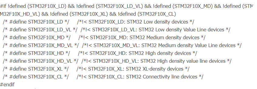
* stm32f10x.h ST 标准头文件 * V3.5.0 版本 * 11-March-2011 2011年3月119 E H$ d) c% d) Y5 S) u * CMSIS Cortex-M3 Device Peripheral Access Layer Header File.(CMSIS:Cortex Microcontroller Software Interface Standard) 是 Cortex-M 处理器系列的与供应商无关的硬件抽象层。 * This file contains all the peripheral register's definitions, bits * definitions and memory mapping for STM32F10x Connectivity line, 1 w& O- `! n& }1 b' \ * High density, High density value line, Medium density, 5 f: K$ p$ [& {. S* O6 [8 k7 u% j w * Medium density Value line, Low density, Low density Value line . e& B' [1 Y4 z; h- T * and XL-density devices. * 这个文件包含了芯片STM32F10X(接口增强型)内部的寄存器定义,位定义,内存地址变换定义,还有一些相应的高密度,低密度产品线的设备。 * The file is the unique include file that the application programmer; y# {% m. X/ D# K6 _$ N% P * is using in the C source code, usually in main.c. This file contains:) |, O* u$ O6 I1 ~! R; } * - Configuration section that allows to select:8 P; y# y2 X; S! L: p M * - The device used in the target application * - To use or not the peripherals drivers in application code(i.e. * code will be based on direct access to peripherals registers * rather than drivers API), this option is controlled by * "#define USE_STDPERIPH_DRIVER" * - To change few application-specific parameters such as the HSE * crystal frequency * - Data structures and the address mapping for all peripherals, F$ }( E, T* D. t0 \9 A& g+ X; G$ B * - Peripheral's registers declarations and bits definition& e' N% j9 M) V& L% Q$ ^- ` * - Macros to access peripheral registers hardware *这个文件在应用程序中是至关重要的头文件,它是用C代码编写而成。通常包括在MAIN主程序中。它包括:1 设备中使用的目标应用程序。 2 决定是否使用外部设备的代码(例如使用基于寄存器的代码,而不是我们所熟悉的API应用程序接口代码)。这一设备可以通过设置 "#define USE_STDPERIPH_DRIVER" 来实现。 3 通过这一文件可以改变诸如外部设备的频率参数。 4 可以了解程序的数据结构以及外设的地址映射。# o/ S. t; L: d) h7 ^/ a 5 外设的寄存器声明和位定义可以在这个文件里面了解到。. F8 Z; u O% ^! h7 s0 O ******************************************************************************1 _( }" v# {+ c4 i) L * @attention1 f/ } S8 j6 ~4 @& H& z/ m * * THE PRESENT FIRMWARE WHICH IS FOR GUIDANCE ONLY AIMS AT PROVIDING CUSTOMERS * WITH CODING INFORMATION REGARDING THEIR PRODUCTS IN ORDER FOR THEM TO SAVE * TIME. AS A RESULT, STMICROELECTRONICS SHALL NOT BE HELD LIABLE FOR ANY7 I% V8 _( R) @) j * DIRECT, INDIRECT OR CONSEQUENTIAL DAMAGES WITH RESPECT TO ANY CLAIMS ARISING * FROM THE CONTENT OF SUCH FIRMWARE AND/OR THE USE MADE BY CUSTOMERS OF THE * CODING INFORMATION CONTAINED HEREIN IN CONNECTION WITH THEIR PRODUCTS.2 k2 c% R7 i. ] *注意:这一文件代码供应给用户,旨在帮助用户提升效率节约时间。ST将不会提供任何对于用户自己代码的解释和帮助。也不会解决其在代码中的任何BUG。! U0 j3 i/ \/ |! O8 D * <h2><center>? COPYRIGHT 2011 STMicroelectronics</center></h2>, m' _( H. z! ^ ******************************************************************************6 I# J$ j, _+ i& \2 g0 M, z* E7 u1 P */ /** @addtogroup CMSIS * @{+ C) X+ } P4 v6 P! X! ? */这个不需要关心,只是说明这个文件的作者,公司产品等等,你贴出来的估计是小小的广而告之,这也是程序员的一点小小的特权嘛6 o* A4 R! O( |- L3 P* W' } /** @addtogroup stm32f10x * @{, R3 M* O3 V5 X */# p, M3 K! T8 r. z $ @3 Y0 L9 q; P #ifndef __STM32F10x_H//如果没有定义__STM32F10x_H ,则定义__STM32F10x_H ; ]9 ?4 R$ E4 z8 s #define __STM32F10x_H. `) ^9 E2 N6 C' c# C% ^ #ifdef __cplusplus// extern "C" {7 P" O/ J6 T8 R2 s3 ? #endif / L9 u9 [" t+ L4 y 这里是一种条件编译。extern "C"指令非常有用,因为C和C++的近亲关系。注意:extern "C"指令中的C,表示的一种编译和连接规约,而不是一种语言。C表示符合C语言的编译和连接规约的任何语言,如Fortran、assembler等。 还有要说明的是,extern "C"指令仅指定编译和连接规约,但不影响语义。例如在函数声明中,指定了extern "C",仍然要遵守C++的类型检测、参数转换规则。 一开始我不解 extern "C" { 这个语句的意思,原来是用来说明后面的定义都是使用C语言写的。这个 __cplusplus 是指C++来的,4、5句的意思就是说如果用C++编译器的话,它里面是定义有__cplusplus 这个的,而通过 extern "C" { 告知编译器,这段代码是用C编写的,要按照C语言编译。这是因为C++里面有函数重载,编译的时候把参数也编译了,而C的话,编译只编译函数名。1 V9 O1 z1 W3 ^ /** @addtogroup Library_configuration_section * @{ *// f6 i* V& u" J9 p0 q" ]3 H ( m& r+ x4 q/ l, | /* Uncomment the line below according to the target STM32 device used in your7 I. \2 q. E0 t C0 S5 r9 V. B9 L: @ application */; D6 r! t3 n: |2 J! ~7 } , N8 U; t$ a% `# D$ Z9 I #if !defined (STM32F10X_LD) && !defined (STM32F10X_LD_VL) && !defined (STM32F10X_MD) && !defined (STM32F10X_MD_VL) && !defined (STM32F10X_HD) && !defined (STM32F10X_HD_VL) && !defined (STM32F10X_XL) && !defined (STM32F10X_CL) /* #define STM32F10X_LD */ /*!< STM32F10X_LD: STM32 Low density devices */& J9 m: v& K- B( y( Y0 x/ l6 ? /* #define STM32F10X_LD_VL */ /*!< STM32F10X_LD_VL: STM32 Low density Value Line devices */ /* #define STM32F10X_MD */ /*!< STM32F10X_MD: STM32 Medium density devices */ /* #define STM32F10X_MD_VL */ /*!< STM32F10X_MD_VL: STM32 Medium density Value Line devices */ /* #define STM32F10X_HD */ /*!< STM32F10X_HD: STM32 High density devices */- I- v* t; `& ~% L /* #define STM32F10X_HD_VL */ /*!< STM32F10X_HD_VL: STM32 High density value line devices */ /* #define STM32F10X_XL */ /*!< STM32F10X_XL: STM32 XL-density devices */2 }; a2 S, E( n& Z2 X /* #define STM32F10X_CL */ /*!< STM32F10X_CL: STM32 Connectivity line devices */ #endif STM32启动文件选择:. y) S7 h& e) K/ B8 d - startup_stm32f10x_ld_vl.s: for STM32 Low density Value line devices - startup_stm32f10x_ld.s: for STM32 Low density devices - startup_stm32f10x_md_vl.s: for STM32 Medium density Value line devices - startup_stm32f10x_md.s: for STM32 Medium density devices - startup_stm32f10x_hd.s: for STM32 High density devices - startup_stm32f10x_xl.s: for STM32 XL density devices - startup_stm32f10x_cl.s: for STM32 Connectivity line devices cl:互联型产品,stm32f105/107系列4 h9 M. W, `2 V1 u1 X2 h vl:超值型产品,stm32f100系列 5 p2 S/ _- T+ }8 }9 K! o( t" x xl:超高密度产品,stm32f101/103系列, v' `" k9 @, Q! @# C ld:低密度产品,FLASH小于64K md:中等密度产品,FLASH=64 or 128+ Z: Q5 P5 W9 H. [7 L! e hd:高密度产品,FLASH大于128 3 r3 W: F; R) N% Z C1 x" w2 b /* Tip: To avoid modifying this file each time you need to switch between these devices, you can define the device in your toolchain compiler preprocessor./ f5 a4 Z: d, F1 L7 k8 j8 f, e- `# ~ 提示:为了避免每次编译都要修改这些文件,意思是可以使用编译器的preprocessor选项来定义芯片型号等,免得反复更新这个文件。...6 G) t+ H4 H8 K; {, z2 i) f1 o" F - Low-density devices are STM32F101xx, STM32F102xx and STM32F103xx microcontrollers; [$ b5 \8 ?. F# E# P8 P6 ]- \( N where the Flash memory density ranges between 16 and 32 Kbytes." s O# W1 Q- Z$ x - Low-density value line devices are STM32F100xx microcontrollers where the Flash memory density ranges between 16 and 32 Kbytes. - Medium-density devices are STM32F101xx, STM32F102xx and STM32F103xx microcontrollers这里定义的是各种产品线的FLASH的大小。 where the Flash memory density ranges between 64 and 128 Kbytes. - Medium-density value line devices are STM32F100xx microcontrollers where the Flash memory density ranges between 64 and 128 Kbytes. 5 R8 P# P3 O8 i* Z, ?' }" f; A( d - High-density devices are STM32F101xx and STM32F103xx microcontrollers where0 |9 u3 ^6 q: M3 Z* V$ A2 o the Flash memory density ranges between 256 and 512 Kbytes.6 v4 F# {6 a Y( a8 F6 _: E4 M - High-density value line devices are STM32F100xx microcontrollers where the Flash memory density ranges between 256 and 512 Kbytes. - XL-density devices are STM32F101xx and STM32F103xx microcontrollers where9 o( }, i# A: D }- C& [% m the Flash memory density ranges between 512 and 1024 Kbytes.5 ~- i4 O% _, G: O$ a! R - Connectivity line devices are STM32F105xx and STM32F107xx microcontrollers." k0 d( V- d6 T6 v */ 2 X! d7 k6 E' W! X; T3 z4 _& R5 | #if !defined (STM32F10X_LD) && !defined (STM32F10X_LD_VL) && !defined (STM32F10X_MD) && !defined (STM32F10X_MD_VL) && !defined (STM32F10X_HD) && !defined (STM32F10X_HD_VL) && !defined (STM32F10X_XL) && !defined (STM32F10X_CL) #error "Please select first the target STM32F10x device used in your application (in stm32f10x.h file)"3 o: Y/ O/ ]0 q8 @8 M #endif 如果设备类型选择不正确,这里会报错的。' H4 ?" C( L8 X o& ]9 j3 x ; K( P- `; N+ a$ {- t) u #if !defined USE_STDPERIPH_DRIVER) T7 e! j4 R i7 O7 \, m: X# f /** G' f" ?) i3 s * @brief Comment the line below if you will not use the peripherals drivers.3 s7 B$ `2 Y4 w6 ]$ e, T In this case, these drivers will not be included and the application code will be based on direct access to peripherals registers */ /*#define USE_STDPERIPH_DRIVER*/* U+ d" Q2 ]# Y- ] #endif /**0 u" k+ @2 X+ {- O7 \* F9 o * @brief In the following line adjust the value of External High Speed oscillator (HSE)+ p$ e2 h8 J2 E4 R& e used in your application Tip: To avoid modifying this file each time you need to use different HSE, you% X! p. w, b; m) p& v can define the HSE value in your toolchain compiler preprocessor. 这些提示:为了避免每次编译都要修改文件,意思是可以使用编译器的preprocessor选项来定义芯片型号等,免得反复更新这个文件。... 1 q; x9 b6 u+ I. M9 _ */ , t' L. J$ O% o #if !defined HSE_VALUE* |; M1 T( o W #ifdef STM32F10X_CL #define HSE_VALUE ((uint32_t)25000000) /*!< Value of the External oscillator in Hz */ #else #define HSE_VALUE ((uint32_t)8000000) /*!< Value of the External oscillator in Hz */ #endif /* STM32F10X_CL */ #endif /* HSE_VALUE */ /** * @brief In the following line adjust the External High Speed oscillator (HSE) Startup Timeout value */①、HSI是高速内部时钟,RC振荡器,频率为8MHz。 ②、HSE是高速外部时钟,可接石英/陶瓷谐振器,或者接外部时钟源,频率范围为4MHz~16MHz。! Q! @. o# @- x6 U ③、LSI是低速内部时钟,RC振荡器,频率为40kHz。 ④、LSE是低速外部时钟,接频率为32.768kHz的石英晶体。 ⑤、PLL为锁相环倍频输出,其时钟输入源可选择为HSI/2、HSE或者HSE/2。倍频可选择为2~16倍,但是其输出频率最大不得超过72MHz。. ?+ y2 I9 k+ ?# a- o. M #define HSE_STARTUP_TIMEOUT ((uint16_t)0x0500) /*!< Time out for HSE start up */ 高速外部时钟启动时间 #define HSI_VALUE ((uint32_t)8000000) /*!< Value of the Internal oscillator in Hz*/$ B+ Y! W5 L* s" b6 M3 @ 外部时钟设置的值 /** * @brief STM32F10x Standard Peripheral Library version number标准外设库版本号的定义 */( k8 C) T/ V5 k& `7 T #define __STM32F10X_STDPERIPH_VERSION_MAIN (0x03) /*!< [31:24] main version */ #define __STM32F10X_STDPERIPH_VERSION_SUB1 (0x05) /*!< [23:16] sub1 version */: c; ~9 }5 x, _" J: E( _- J- y/ H #define __STM32F10X_STDPERIPH_VERSION_SUB2 (0x00) /*!< [15:8] sub2 version */, ?, D8 O0 ?- B% x #define __STM32F10X_STDPERIPH_VERSION_RC (0x00) /*!< [7:0] release candidate */ 8 H% `5 J! s+ H+ n2 l% j3 E #define __STM32F10X_STDPERIPH_VERSION ( (__STM32F10X_STDPERIPH_VERSION_MAIN << 24)\ |(__STM32F10X_STDPERIPH_VERSION_SUB1 << 16)\ |(__STM32F10X_STDPERIPH_VERSION_SUB2 << 8)\! z) {) r/ E% F% k2 ^, l |(__STM32F10X_STDPERIPH_VERSION_RC)) , x$ {3 `1 A6 s* \7 A /** * @} */. O, i' V8 o; e / E, A. f2 d4 Y4 m0 q7 ?. Y /** @addtogroup Configuration_section_for_CMSIS * @{ */ /**5 L7 [1 q, Q- B( C& b. v* N * @brief Configuration of the Cortex-M3 Processor and Core Peripherals 配置Cortex-M3处理器和核内外设) J' q$ N. b( M/ i */3 T9 Z+ L2 l( ~/ q #ifdef STM32F10X_XL! D8 P" F ^4 L% o #define __MPU_PRESENT 1 /*!< STM32 XL-density devices provide an MPU */ #else #define __MPU_PRESENT 0 /*!< Other STM32 devices does not provide an MPU */. ^( F0 M" l3 l# R, m, ] #endif /* STM32F10X_XL */) R% e& B$ w) x5 O #define __NVIC_PRIO_BITS 4 /*!< STM32 uses 4 Bits for the Priority Levels */ #define __Vendor_SysTickConfig 0 /*!< Set to 1 if different SysTick Config is used */ /**# [- t% Y" `( B0 h1 O* } * @brief STM32F10x Interrupt Number Definition, according to the selected device % [$ J' p3 U9 K. _4 f * in @ref Library_configuration_section 中断线定义,前部分对于所有STM32F10x都有相同定义,后部分根据不同器件容量采用条件编译定义不同中断线。9 _6 Q) F" X, b, @2 a1 V U */ 这里是STM32比较重要的头文件 $ Q% p% z4 \7 \( B7 }: D
外设中断ID:
这里是STM32比较重要的头文件
外设中断ID:
#ifdef STM32F10X_MD_VL這是我們前面講過的不同的芯片型號,對應 著不同的中斷級別。請大家自行研究! . {; x7 }6 |8 U: e" q! _5 x
, S. d# }/ l3 S. _) B+ ?. F7 i7 D
#include "core_cm3.h"STM32的内核是ARM CORTEX-M3,这个core_cm3.h包含的是一些内核相关的函数和宏定义,例如核内寄存器定义、部分核内外设的地址等等,其对应的是core_cm3.c文件。初学可以不管他,只要把它包含进工程里就行了,这里都是非常底层的函数,上层的一些函数直接调用它们了。如果对CORTEX-M3内核有兴趣或者基础较高,想深入了解这些函数,可以仔细研读一下,我们在后续的开讲中会仔细讲解这一个文件的内容。 #include "system_stm32f10x.h"这个文件就是我们现在所讲的文件了。 #include <stdint.h><stdint.h> 定义了 int16_t 、 uint32_t 、 int64_t 等整型,在需要确定大小的整型时可以使用它们代替 short 、 unsigned long long 等,在 C 整型中,只使用 int 。' {7 b- \* c0 D' U3 O8 [4 p /** @addtogroup Exported_types- K- |6 j% ~9 C2 t * @{ */ 1 [' M' [# O7 t, _1 I % t4 `% O; G: @ /*!< STM32F10x Standard Peripheral Library old types (maintained for legacy purpose) */由于新的文件与老的文件会有不兼容问题,所以要转换变量类型。1 ]' v/ _3 t5 u6 Q typedef int32_t s32; typedef 在计算机编程语言中用来为复杂的声明定义简单的别名,与宏定义有些差异。它本身是一种存储类的关键字,与auto、extern、mutable、static、register等关键字不能出现在同一个表达式中。 《变量类型》,3.0以后的版本中使用了CMSIS数据类型,变量的定义有所不同,但是出于兼容旧版本的目的,以上的数据类型仍然兼容。 CMSIS IO类型限定词
件库与CMSIS数据类型对比
stm32f10x.h文件中还包含了常用的布尔形变量定义,如:* K* n! u! R8 G+ h8 J8 M 1 typedef enum {RESET = 0, SET = !RESET} FlagStatus, ITStatus; 2 $ E* W% v) y+ t; ~/ I& a% e' \ 3 typedef enum {DISABLE = 0, ENABLE = !DISABLE} FunctionalState;8 K8 `8 l2 j8 M+ }( t4 k- r 4 8 {9 i. L9 ^/ x* r9 P7 q 5 #define IS_FUNCTIONAL_STATE(STATE) (((STATE) == DISABLE) || ((STATE) == ENABLE)) 6 7 M4 Z I$ w! _; w1 S2 Q( M; I 7 typedef enum {ERROR = 0, SUCCESS = !ERROR} ErrorStatus; 不同版本的标准外设库的变量定义略有不同,如3.4版本中就没有之前版本的TRUE和FALSE的定义,用户也可以根据自己的需求按照上面的格式定义自己的布尔形变量。在使用标准外设库进行开发遇到相关的定义问题时应首先找到对应的头文件定义。 typedef int16_t s16; typedef int8_t s8;. J5 ^7 h" y' K typedef const int32_t sc32; /*!< Read Only */ const是一个C语言的关键字,它限定一个变量不允许被改变。使用const在一定程度上可以提高程序的安全性和可靠性。另外,在观看别人代码的时候,清晰理解const所起的作用,对理解对方的程序也有一些帮助。另外CONST在其他编程语言中也有出现,如C++、PHP5、C#.net、HC08 C。 typedef const int16_t sc16; /*!< Read Only */1 x$ n* O6 w$ B( |3 Z" h typedef const int8_t sc8; /*!< Read Only */ * U9 R- x s/ t* ? U; i3 v3 } typedef __IO int32_t vs32; typedef __IO int16_t vs16;% a; \6 m2 [! T3 A8 F* F1 n typedef __IO int8_t vs8;0 i/ c5 a! @* U* k9 k typedef __I int32_t vsc32; /*!< Read Only */ typedef __I int16_t vsc16; /*!< Read Only */ typedef __I int8_t vsc8; /*!< Read Only */ typedef uint32_t u32; typedef uint16_t u16; typedef uint8_t u8; 5 u a. J5 _* g$ [5 F typedef const uint32_t uc32; /*!< Read Only */5 }/ b2 B, K2 b# Y7 u/ C, \+ f- j typedef const uint16_t uc16; /*!< Read Only *// Z& a* J; b C V7 v6 e# j typedef const uint8_t uc8; /*!< Read Only */ typedef __IO uint32_t vu32; typedef __IO uint16_t vu16;, x+ l2 a; [5 }7 ]& x! |' w typedef __IO uint8_t vu8; ; Q) Z1 D7 |9 i1 T: J# I typedef __I uint32_t vuc32; /*!< Read Only */- B# Y0 H' N* L8 F typedef __I uint16_t vuc16; /*!< Read Only */1 N/ c' F& k4 d typedef __I uint8_t vuc8; /*!< Read Only */$ w: X9 |3 u. K" ?/ T7 }0 g typedef enum {RESET = 0, SET = !RESET} FlagStatus, ITStatus; L$ g1 m3 h% g* V) {. B4 I+ g typedef enum {DISABLE = 0, ENABLE = !DISABLE} FunctionalState;& c& `( C( r; N #define IS_FUNCTIONAL_STATE(STATE) (((STATE) == DISABLE) || ((STATE) == ENABLE)) - w+ b b( K, { typedef enum {ERROR = 0, SUCCESS = !ERROR} ErrorStatus; /*!< STM32F10x Standard Peripheral Library old definitions (maintained for legacy purpose) */ 由于新的文件与老的文件会有不兼容问题,所以要转换变量类型。 2 X7 A# ]5 P! a, Z7 l$ Z #define HSEStartUp_TimeOut HSE_STARTUP_TIMEOUT 请大家注意这里的定义,高速外设时钟的启动时间。. | O: c& F8 l) m #define HSE_Value HSE_VALUE+ s% s. U. d q- Z0 @) j #define HSI_Value HSI_VALUE /** * @}* I6 q3 v" |! d7 V& ~- ?4 s */4 B" Q( O8 j( S/ L! S1 K: s / N' L! [3 [. }$ @% @* b /** @addtogroup Peripheral_registers_structures5 ~2 z0 F6 A! h: a% q! C * @{ */ /** * @brief Analog to Digital Converter */ typedef struct ADC_TypeDef结构体的声名,看看它内部都有哪些内容。请读者注意。 ADC_TypeDef,看起来是一个结构类型,是对ADC寄存器各地址的一个定义。) A! }3 w+ W5 F# d1 E6 S p {__IO就是volatileuint32_t就是32位无符号整形数。 这都是ARM公司无聊滴在CMSIS库里面定义的。STM32库1.x 2.x都没有这玩意,到了3.0以后引入了CMSIS就有了。 __IO uint32_t SR; __IO uint32_t CR1; __IO uint32_t CR2; __IO uint32_t SMPR1;! j4 m' I( c3 @1 h$ O( d ~ __IO uint32_t SMPR2;4 h) K- f" n% ] ^ __IO uint32_t JOFR1;+ g+ s) Y% e& p# [ __IO uint32_t JOFR2; __IO uint32_t JOFR3;; V- l, y: t' I% @! c# F __IO uint32_t JOFR4; __IO uint32_t HTR;/ x3 |! r* }( D5 d W __IO uint32_t LTR; __IO uint32_t SQR1; __IO uint32_t SQR2; __IO uint32_t SQR3;$ V) \9 i: g) @ __IO uint32_t JSQR;" ^; U# E" Q; h& X __IO uint32_t JDR1; __IO uint32_t JDR2; __IO uint32_t JDR3; __IO uint32_t JDR4; __IO uint32_t DR;, X I7 Y; o$ b } ADC_TypeDef; /** % b' W# \5 r& J" B2 h/ ^ * @brief Backup Registers 3 `, R- q# e* d2 V3 D' `6 g. N; F# B */( ]* a7 v Y, h4 g" f: H6 H typedef struct 这个结构体声明的是数据备份寄存器,它们是16位的。它可以管理防范入侵,可以存储RTC检验值,可以做数据备份。1 g3 _3 t2 Y/ |9 n0 ?# } {5 h( n% B2 o8 Q& l4 ?: R uint32_t RESERVED0; __IO uint16_t DR1; DR代表数据备份1---45 uint16_t RESERVED1;' Z& h H. Y v+ v __IO uint16_t DR2; uint16_t RESERVED2; c$ g7 ^: J% v# t. c __IO uint16_t DR3;/ H2 g' s, C9 q uint16_t RESERVED3;+ m2 ` J g1 A, V3 @( N I _ __IO uint16_t DR4; uint16_t RESERVED4;- N |0 D7 X8 S5 s( s' b, G __IO uint16_t DR5;2 U; G) n* x" d, E! n& N uint16_t RESERVED5; G$ b' U- M: Q& U }. w4 w% K __IO uint16_t DR6; uint16_t RESERVED6;/ ^( L/ W* S) h __IO uint16_t DR7;9 A) Z8 ? t9 w+ z8 E# z- g E uint16_t RESERVED7;$ F w4 Y; H) t3 F- Z4 W6 Y" I0 S& C6 W __IO uint16_t DR8; uint16_t RESERVED8; __IO uint16_t DR9;& F" V4 B! J: t( B9 ^2 V& x uint16_t RESERVED9; __IO uint16_t DR10;5 `1 ~0 ~2 g/ j* p9 i; l- ~6 S uint16_t RESERVED10; __IO uint16_t RTCCR; RTC时钟校准寄存器 uint16_t RESERVED11;- o5 R' Z/ R. ~2 ] __IO uint16_t CR; CR备份控制寄存器/ D0 U( t+ o/ N. g* g0 p uint16_t RESERVED12;8 ?, X- p+ R% l( E0 i/ d3 s1 m __IO uint16_t CSR; CSR 备份控制状态寄存器 1 d- c( Z$ a `' R+ V* E uint16_t RESERVED13[5]; __IO uint16_t DR11; uint16_t RESERVED14; __IO uint16_t DR12;/ c$ V; A* O1 ?4 U1 _! L# t# M uint16_t RESERVED15;' Z$ Z% K- F2 K: `! | __IO uint16_t DR13;2 F. I. ]; ]# r uint16_t RESERVED16;/ e. {; H1 i n, o7 N __IO uint16_t DR14; uint16_t RESERVED17;' M; c% y* O1 \) l; a __IO uint16_t DR15;8 c" m. T) a1 e0 A3 }* j uint16_t RESERVED18;" L/ h6 }7 d# W7 N% q2 V- f) Q __IO uint16_t DR16; uint16_t RESERVED19; __IO uint16_t DR17;% W- S6 r" q, R0 P) I1 [ uint16_t RESERVED20; Y! q7 n( K5 g, s __IO uint16_t DR18;1 c; T* ^! W! e5 g4 U" I) n uint16_t RESERVED21;# p1 F! W; |! B' H' Z8 ^( c __IO uint16_t DR19;2 u4 L1 W- M5 E uint16_t RESERVED22;3 h; [8 h* Z% N! j% ~. b" d __IO uint16_t DR20;( H" h4 W1 g) y1 b5 R- b uint16_t RESERVED23; m& l% i2 Z- B __IO uint16_t DR21;( _5 W# e, w2 A2 W uint16_t RESERVED24;% g+ M$ l2 P. P: H8 @! L" \ __IO uint16_t DR22; uint16_t RESERVED25; __IO uint16_t DR23; uint16_t RESERVED26; __IO uint16_t DR24;/ _ w8 I3 _( h/ U uint16_t RESERVED27; s% }! }( b% f" c- H f# O* \4 V$ t __IO uint16_t DR25;2 [8 A9 P6 `* j2 s6 [/ z7 b uint16_t RESERVED28; __IO uint16_t DR26; uint16_t RESERVED29;6 j2 B! s8 {5 V2 l1 J __IO uint16_t DR27;* U. f3 |9 t' v! ^ e uint16_t RESERVED30; __IO uint16_t DR28; uint16_t RESERVED31;0 l2 _# O1 D- q1 z% Q __IO uint16_t DR29; uint16_t RESERVED32;0 \7 k5 Y. e. Q: x8 O% H6 `6 N" t9 f. u __IO uint16_t DR30;4 C3 O- _3 L! D3 e uint16_t RESERVED33; __IO uint16_t DR31; uint16_t RESERVED34;3 L- x V8 P3 j) G/ A+ P! O$ I __IO uint16_t DR32; uint16_t RESERVED35; __IO uint16_t DR33; uint16_t RESERVED36;2 x' h* n/ c9 J! E2 y# f __IO uint16_t DR34;4 o) L! k2 J5 N, b6 { uint16_t RESERVED37; __IO uint16_t DR35;! M% J* {8 s; } uint16_t RESERVED38; __IO uint16_t DR36; uint16_t RESERVED39; __IO uint16_t DR37;3 y* Y8 R X! t' M8 ~+ t( S2 N uint16_t RESERVED40; __IO uint16_t DR38; uint16_t RESERVED41;2 ?# s+ B1 i& ]9 T! Q __IO uint16_t DR39;9 M: F; h7 o3 T! A9 B uint16_t RESERVED42; __IO uint16_t DR40;* E& t; V) V5 m* Z* s" a uint16_t RESERVED43; __IO uint16_t DR41; uint16_t RESERVED44;( ?& @( U" U& F7 F2 T+ F2 [% W __IO uint16_t DR42;$ b. n0 ^3 x" k! S) V: v) a uint16_t RESERVED45; } BKP_TypeDef; + }: p) S: N$ J /** 2 J4 U# R8 N; r/ d, _3 N * @brief Controller Area Network TxMailBox 8 B) U* X" A( m9 ? */ typedef struct2 e& g c! o- |. u7 W! z: P! f: b { __IO uint32_t TIR;1 k( {0 M; P. ?! n( v __IO uint32_t TDTR; __IO uint32_t TDLR; __IO uint32_t TDHR;5 x5 X3 X O- m# b4 B" `' Y6 J } CAN_TxMailBox_TypeDef; CAN的发送邮箱寄存器的结构体定义。 /** ' b4 d4 R6 c8 E$ V6 X' W5 c * @brief Controller Area Network FIFOMailBox */% Y9 J* u- Q/ I: f9 T, O , l3 C" N" u4 [! Q9 d typedef struct9 f& G2 _6 L& j6 F {$ U+ `# f3 y& ?0 L0 f3 v __IO uint32_t RIR;9 `% T0 U7 l: u; o __IO uint32_t RDTR; __IO uint32_t RDLR;" V# i$ q! E2 H) E2 g- ` __IO uint32_t RDHR;2 j' A+ p+ B6 R+ Y! P } CAN_FIFOMailBox_TypeDef;先进先出(FIFO)缓冲器,是一种寄存器。在这个头文件里定义了它的结构体类型。 /** * k0 X1 U/ ` [. ?/ y/ h * @brief Controller Area Network FilterRegister */ typedef struct { __IO uint32_t FR1;& J. {, i$ `; D7 X __IO uint32_t FR2;, ^- h9 Q& _$ n+ H/ p) @. q1 Z }CAN_Filter Register_TypeDef;CAN硬件过滤器工作模式、访问码和访问码掩码。 通过设置CAN过滤器,可以使CAN端口只接收符合规定的的CAN数据包,这样就能将CAN总线划分成若干网段用于支持不同应用。 - R) W/ d+ H: @4 Z9 P% d# p0 v0 C0 n/** # Q. Z" ~" i! J' M * @brief Controller Area Network */ typedef struct+ M1 H4 a( z. t! m {, n2 y+ A. R4 O5 F q$ {* j% p8 @ __IO uint32_t MCR;! O" b7 b& l1 q% R5 z+ c1 R+ x' j __IO uint32_t MSR; __IO uint32_t TSR; __IO uint32_t RF0R;: d- o' Y! X0 D) } __IO uint32_t RF1R; __IO uint32_t IER;' I4 p+ v8 J/ {5 o! X' d __IO uint32_t ESR;( X- ^. p j% a: S5 `+ L2 ` __IO uint32_t BTR; uint32_t RESERVED0[88]; CAN_TxMailBox_TypeDef sTxMailBox[3]; CAN_FIFOMailBox_TypeDef sFIFOMailBox[2];- n. ]" S9 Z! q uint32_t RESERVED1[12]; __IO uint32_t FMR; __IO uint32_t FM1R; uint32_t RESERVED2; __IO uint32_t FS1R; uint32_t RESERVED3; __IO uint32_t FFA1R; uint32_t RESERVED4;: u+ y. u' T1 ~# S __IO uint32_t FA1R; uint32_t RESERVED5[8]; #ifndef STM32F10X_CL CAN_FilterRegister_TypeDef sFilterRegister[14]; #else CAN_FilterRegister_TypeDef sFilterRegister[28];# D- m% N) c: _6 a #endif /* STM32F10X_CL */ } CAN_TypeDef;2 T) b$ B: Q, u& _ % E2 T* L" R% Z0 v' D9 j- p /** * @brief Consumer Electronics Control (CEC) */* I& o7 r7 t# B6 u6 O/ h; O+ K# S typedef struct {6 [; [/ d8 f3 }: T% ] __IO uint32_t CFGR;/ j; d$ Y3 M0 S& o' v0 [ __IO uint32_t OAR;1 s% S, x4 ~! N* ^8 b __IO uint32_t PRES; __IO uint32_t ESR; __IO uint32_t CSR; __IO uint32_t TXD; __IO uint32_t RXD; 9 y/ F) r8 s4 ? } CEC_TypeDef; CEC用于记录CAN总线发送数据错误的计数器% |# ~& O8 {/ H( f% z $ r/ U! C5 {: C0 `0 g, n! x /** # H4 R _! n {' @ * @brief CRC calculation unit : E8 d& }- }6 [/ ^2 V. I! P( p0 o, B */) g! z& j0 `9 f) x : H0 E L, d | typedef struct5 F5 m' Y& _/ q3 d3 Y+ y. s1 s { __IO uint32_t DR; __IO uint8_t IDR;0 e: ?) A: |0 m a( ~( B uint8_t RESERVED0; uint16_t RESERVED1;, o& d$ l6 G; e" S __IO uint32_t CR;+ P3 g8 `" @! M; Y5 P/ U } CRC_TypeDe CRC校验 /** * @brief Digital to Analog Converter 数模转换相应的结构体,DAC相关寄存器啊( Y6 ~: n5 T# S& Y- R" p; w$ a$ l */ # e- `; m f3 G! S, g2 H typedef struct' k8 O) |$ @& V9 R& j {1 k2 I# O+ m3 l, r; `+ r2 r+ Z! Y$ s __IO uint32_t CR;8 f$ w/ Q4 @2 n8 \+ U __IO uint32_t SWTRIGR; SWTRIGR 这个DAC软件触发寄存器 __IO uint32_t DHR12R1; DAC 通道 1 的 12 位右对齐数据保持寄存器:DAC_DHR12R1。这个我只讲一个,这里面全部是关于DAC转换的相关寄存器。请大家自行对照硬件手册查找。 __IO uint32_t DHR12L1;- l3 d! Z9 Q/ e t4 w) Z& X9 q w __IO uint32_t DHR8R1; __IO uint32_t DHR12R2;( P! Z6 \7 b" u9 R- i0 v3 z' @# ?8 T __IO uint32_t DHR12L2; __IO uint32_t DHR8R2; __IO uint32_t DHR12RD;9 V1 Q, v; N! y$ i. B __IO uint32_t DHR12LD; __IO uint32_t DHR8RD;2 {, I( `/ a1 A8 R9 ^ ^ __IO uint32_t DOR1;- d8 P2 k! F! ~0 p5 }9 M5 q$ |& } __IO uint32_t DOR2; #if defined (STM32F10X_LD_VL) || defined (STM32F10X_MD_VL) || defined (STM32F10X_HD_VL)" R8 }* u/ e" L; X8 H# {) e* g. s __IO uint32_t SR; #endif: a* F" u7 H! m1 R3 x, ` } DAC_TypeDef; /** * @brief DMA Controller DMA 传输将数据从一个地址空间复制到另外一个地址空间。当CPU 初始化这个传输动作,传输动作本身是由 DMA 控制器来实行和完成。典型的例子就是移动一个外部内存的区块到芯片内部更快的内存区。像是这样的操作并没有让处理器工作拖延,反而可以被重新排程去处理其他的工作。DMA 传输对于高效能 嵌入式系统算法和网络是很重要的。 DMA 在实现DMA传输时,是由DMA控制器直接掌管总线,因此,存在着一个总线控制权转移问题。即DMA传输前,CPU要把总线控制权交给DMA控制器,而在结束DMA传输后,DMA控制器应立即把总线控制权再交回给CPU。一个完整的DMA传输过程必须经过DMA请求、DMA响应、DMA传输、DMA结束4个步骤。 */0 N* T" m; f" O, k3 w0 G% p typedef struct 这里就是直接内存寻址寄存器相关定义,我想DMA大家应该不是太陌生。 {% L$ h) m8 O$ }! d __IO uint32_t CCR;# N& d6 D& L0 v( w4 Z8 n __IO uint32_t CNDTR;) Q" k& v4 ]: W' o4 v6 v; e __IO uint32_t CPAR;6 Z2 d& A9 O/ h' S __IO uint32_t CMAR;* `2 c! `( [, V, b) H( m* x } DMA_Channel_TypeDef; $ w" i% G+ U) I- l typedef struct1 |6 u. A, ?4 r {! ~# N& y0 \- v i; h __IO uint32_t ISR; __IO uint32_t IFCR; } DMA_TypeDef; /** * @brief Ethernet MAC */ MAC(Medium Access Control)模块,实现符合 IEEE 802.3 标准的 MAC 逻辑。 这个结构体是网络模块的相关定义。 8 w5 E' c, {" j6 R% g b+ a" D typedef struct {% e8 B0 o: s$ G& f __IO uint32_t MACCR;, ~: A5 s: B$ X5 D' C __IO uint32_t MACFFR; __IO uint32_t MACHTHR;8 K0 l2 N, @3 V" z3 a+ }% J" p __IO uint32_t MACHTLR;0 @6 F/ p, L* S5 y __IO uint32_t MACMIIAR;) ~1 r# u3 X, f, m- _$ r* q% _* F __IO uint32_t MACMIIDR; __IO uint32_t MACFCR; __IO uint32_t MACVLANTR; /* 8 */ uint32_t RESERVED0[2];4 `" z2 _/ [+ D0 K$ ~; Q3 O __IO uint32_t MACRWUFFR; /* 11 */5 n! Q- ?9 j1 m$ ?$ y8 u! B6 \ __IO uint32_t MACPMTCSR;2 D' Z- U9 _# B/ n4 |+ k uint32_t RESERVED1[2]; __IO uint32_t MACSR; /* 15 */) u, z& g9 {5 ? __IO uint32_t MACIMR; __IO uint32_t MACA0HR;8 o2 [+ Q9 j. |4 y& P! @ __IO uint32_t MACA0LR;2 b' Y( q0 w9 S, x9 ~ P# V. | __IO uint32_t MACA1HR;7 ?4 B, u& \# Z4 b! _5 H9 u6 D __IO uint32_t MACA1LR; __IO uint32_t MACA2HR;( i( z2 _' [: S1 p" R- T8 { __IO uint32_t MACA2LR;. F& k5 c/ r M x* B( L- H( B- Q __IO uint32_t MACA3HR; __IO uint32_t MACA3LR; /* 24 */ uint32_t RESERVED2[40];9 [7 K. _/ b! _! T# ] __IO uint32_t MMCCR; /* 65 */ __IO uint32_t MMCRIR; __IO uint32_t MMCTIR; __IO uint32_t MMCRIMR;# F. o3 z0 J0 o9 G5 I __IO uint32_t MMCTIMR; /* 69 */0 L+ m# ]$ L" o; Q uint32_t RESERVED3[14];" j9 X* u. g3 W __IO uint32_t MMCTGFSCCR; /* 84 */ __IO uint32_t MMCTGFMSCCR;4 B8 h' _$ W# E) V" _( E. U uint32_t RESERVED4[5]; __IO uint32_t MMCTGFCR; uint32_t RESERVED5[10]; __IO uint32_t MMCRFCECR; __IO uint32_t MMCRFAECR; uint32_t RESERVED6[10];# g" i5 @& t5 Q& B8 q __IO uint32_t MMCRGUFCR;' _% H, o" {" g! \. @ uint32_t RESERVED7[334];5 x, j \( K0 J0 t __IO uint32_t PTPTSCR; __IO uint32_t PTPSSIR;( N& f- Q/ f! h; `0 K2 d; @ __IO uint32_t PTPTSHR;" n. Z0 |6 G6 R( Z8 C __IO uint32_t PTPTSLR;% Q, A. i* L" Q1 K! H9 B& C" A8 | __IO uint32_t PTPTSHUR; __IO uint32_t PTPTSLUR;2 ?5 X' _! Q, q8 K+ Y/ K; Q, V __IO uint32_t PTPTSAR; __IO uint32_t PTPTTHR; H6 d$ h5 Z r& \6 D. I# K __IO uint32_t PTPTTLR; uint32_t RESERVED8[567]; __IO uint32_t DMABMR;8 K. m2 Z6 T' `( K2 O __IO uint32_t DMATPDR; __IO uint32_t DMARPDR; __IO uint32_t DMARDLAR; __IO uint32_t DMATDLAR;0 q& @7 M8 C2 P0 O __IO uint32_t DMASR;0 F! C6 H6 x* ?+ c" E' { __IO uint32_t DMAOMR;0 d% ]- t1 }' e( ~* ~3 y; y6 V __IO uint32_t DMAIER;! N5 }7 W3 `1 N8 a @ __IO uint32_t DMAMFBOCR; uint32_t RESERVED9[9]; __IO uint32_t DMACHTDR; __IO uint32_t DMACHRDR; __IO uint32_t DMACHTBAR; __IO uint32_t DMACHRBAR;5 ]8 x4 P F F7 ?( y/ {# D$ f } ETH_TypeDef; / Z, l3 h9 |. J2 N: } /** ' E- k# D& m3 n* X * @brief External Interrupt/Event Controller2 ^% L( i% l) q# ^+ E */ EXTI寄存器结构 6 r0 I& j4 ]& h( L7 F; FEXTI 寄存器结构,EXTI_TypeDef,在文件stm2f10x_map.h中定义如下: typedef struct { vu32 IMR; vu32 EMR; vu32 RTSR; vu32 FTSR; vu32 SWIER; vu32 PR; }EXTI_TypeDef; Table 128. 例举了EXTI 所有寄存器 Table 128. EXTI寄存器 寄存器 描述 IMR 中断屏蔽寄存器 EMR 事件屏蔽寄存器 RTSR 上升沿触发选择寄存器 FTSR 下降沿触发选择寄存器 SWIR 软件中断事件寄存器 PR 挂起寄存器 typedef struct- V/ |& ]/ Q0 K+ x0 _ { " d6 R8 T6 P' V6 ^ g; ^ __IO uint32_t IMR;& T+ t8 B( A% x9 f* B9 L$ g; S __IO uint32_t EMR; __IO uint32_t RTSR;9 O% L7 }! l6 K' k' Z/ J __IO uint32_t FTSR;) F$ w7 V+ ]5 G4 X" X __IO uint32_t SWIER;' m8 t) @( `5 |2 H7 _! ] __IO uint32_t PR; } EXTI_TypeDef; /** * @brief FLASH Registers& J; }5 L0 L. _1 \6 e! Q0 N+ S- \ */ FLASH寄存器 寄存器 描述 ACR FLASH访问控制寄存器 KEYR FPEC密钥寄存器 OPTKEYR 选择字节密钥寄存器 SR FLASH状态寄存器 CR FLASH控制寄存器 AR FLASH地址寄存器 OBR 选择字节和状态寄存器 WRPR 选择字节写保护寄存器 typedef struct# p, v2 o/ \% k @* q1 m& @* M/ S { __IO uint32_t ACR; __IO uint32_t KEYR; __IO uint32_t OPTKEYR; __IO uint32_t SR; __IO uint32_t CR;3 e& O! E! j. n' `. ` __IO uint32_t AR; __IO uint32_t RESERVED; __IO uint32_t OBR; __IO uint32_t WRPR; #ifdef STM32F10X_XL uint32_t RESERVED1[8]; __IO uint32_t KEYR2;$ I9 G W) i* b) Y uint32_t RESERVED2; - `' z: x5 [) x4 Q9 A9 y __IO uint32_t SR2; __IO uint32_t CR2; __IO uint32_t AR2; " \+ [, G& ~2 D6 S! ^; W5 ?) n #endif /* STM32F10X_XL */ } FLASH_TypeDef;5 X+ H: v' N/ l8 V* {
*************************************************** //本程序只供学习使用,如果用于工程应用,请仔细检查: B3 a, c, t6 I' {6 { //主要对于ST公司的库存文件stm32f10x.h进行解析2 Q% N2 A8 d$ l9 x& I //修改日期:2014/6 //Copyright(C) 2014-2025 //All rights reserved4 c- z' s8 [$ y* t //******************************************************************************** */2 E2 }* ?/ i u* I$ P0 ~ /** * @brief Real-Time Clock2 j: a; ]3 r1 b6 H7 v, [6 _" d( m */8 o3 C6 }9 E. K3 D6 q RTC预分频器余数寄存器高位(RTC_DIVH) RTC预分频器余数寄存器低位(RTC_DIVL) RTC控制寄存器高位(RTC_CRH) RTC控制寄存器低位(RTC_CRL) RTC预分频装载寄存器高位(RTC_PRLH) 0 f$ C n7 k: o' F RTC预分频装载寄存器低位(RTC_PRLL) RTC计数器寄存器高位(RTC_CNTH); ~: \8 e% a2 W( }4 \" H. t RTC计数器寄存器低位(RTC_CNTL) RTC闹钟寄存器高位(RTC_ALRH) RTC闹钟寄存器低位(RTC_ALRL) 8 S1 z4 V) f) @/ A z typedef struct { __IO uint16_t CRH; uint16_t RESERVED0; RTC寄存器是16位可寻址寄存器,这是定义它的数据类型为16位的。 __IO uint16_t CRL; uint16_t RESERVED1;5 L8 _8 [$ b: [ c; _5 x __IO uint16_t PRLH; uint16_t RESERVED2; __IO uint16_t PRLL;: i0 T2 b: I4 `; A) t+ z2 u. Z+ h5 h uint16_t RESERVED3; __IO uint16_t DIVH;0 b! |. l( [# s+ ?. `7 K uint16_t RESERVED4; __IO uint16_t DIVL;4 ]1 J# V0 x% J/ ?8 O uint16_t RESERVED5;* |: L0 G: w1 M __IO uint16_t CNTH;( m z/ I9 C7 r uint16_t RESERVED6;' s( M9 r. c) A& [8 n" i/ Q __IO uint16_t CNTL; uint16_t RESERVED7;( w+ z1 E) }6 N- s __IO uint16_t ALRH;8 v* ]7 E. Y. j8 a U# D( ?5 Z uint16_t RESERVED8;4 s: z/ t, U- w5 I __IO uint16_t ALRL; uint16_t RESERVED9; } 0 G; l6 J' D! W9 z1 I# Z+ Z RTC_TypeDef; ' ^% _1 z3 {3 q0 t! p- v0 {: U /** ' @* `) Z6 G) L% @% \" [ * @brief SD host Interface SD卡接口 */ SDIO电源控制寄存器(SDIO_POWER) SDIO时钟控制寄存器(SDIO_CLKCR) ) `0 S) ^( t) d& B SDIO参数寄存器(SDIO_ARG) SDIO命令寄存器(SDIO_CMD) SDIO命令响应寄存器(SDIO_RESPCMD) SDIO响应1..4寄存器(SDIO_RESPx) 4 s& Q9 D) h$ X) n* w SDIO数据定时器寄存器(SDIO_DTIMER) SDIO数据长度寄存器(SDIO_DLEN)2 Q9 `9 l" ]$ k$ i- {! A3 k4 S SDIO数据控制寄存器(SDIO_DCTRL)& \* B+ C, S2 D; B0 ? SDIO数据计数器寄存器(SDIO_DCOUNT) V8 r+ `+ N3 ?- [4 _ SDIO状态寄存器(SDIO_STA) 5 ?/ h! T0 w- P# G; E' k SDIO清除中断寄存器(SDIO_ICR) # U( k W+ Y: x) f- ] SDIO中断屏蔽寄存器(SDIO_MASK)7 }6 F+ ?* P8 d+ Q; d SDIO FIFO计数器寄存器(SDIO_FIFOCNT)# N; t* T% u8 d( l! ] SDIO数据FIFO寄存器(SDIO_FIFO) typedef struct; j/ D( f3 O$ m1 t* i { __IO uint32_t POWER; __IO uint32_t CLKCR; __IO uint32_t ARG; __IO uint32_t CMD;' g5 }9 O& Q7 w' m7 ?6 ` __I uint32_t RESPCMD;) L' C" T( r: Z0 S+ @ __I uint32_t RESP1; __I uint32_t RESP2; __I uint32_t RESP3; __I uint32_t RESP4; __IO uint32_t DTIMER; __IO uint32_t DLEN; __IO uint32_t DCTRL;- Z# ~, h- Z. Y __I uint32_t DCOUNT; __I uint32_t STA;) h" Q) j5 f7 j$ \ __IO uint32_t ICR; __IO uint32_t MASK;- ]/ @0 x& ?3 Y; C& @ uint32_t RESERVED0[2];$ E7 x! R' R+ K) }, w __I uint32_t FIFOCNT;8 m1 W% @5 D) C: K2 h; Y" W uint32_t RESERVED1[13]; __IO uint32_t FIFO;$ f; c5 w0 f) m5 R8 n( E2 ^ } SDIO_TypeDef; 9 U" x. K( M& }1 A /** 7 r! t; L9 y: M+ K, [0 S * @brief Serial Peripheral Interface-------------SPI串行总线" @* I* M& x! I: h$ v */; A* {) x7 _6 }( Q/ O SPI控制寄存器1(SPI_CR1) SPI控制寄存器2(SPI_CR2) SPI 状态寄存器(SPI_SR) ' K i% W3 N1 h" J' ~ SPI 数据寄存器(SPI_DR) SPI CRC多项式寄存器(SPI_CRCPR) Y. H) [4 ^# U- P5 |9 w0 k SPI Rx CRC寄存器(SPI_RXCRCR) SPI Tx CRC寄存器(SPI_TXCRCR) ( Y$ n/ v0 _, x- w- M2 E SPI_I2S配置寄存器(SPI_I2S_CFGR) SPI_I2S预分频寄存器(SPI_I2SPR) - G. n4 ^4 C2 b5 p& X . r* ~4 i7 C, N+ r* o typedef struct { __IO uint16_t CR1; uint16_t RESERVED0; __IO uint16_t CR2;+ q) z+ i4 O: i; \8 l uint16_t RESERVED1;0 N7 B$ G2 s: K% V0 m& K- Y- e* p __IO uint16_t SR; uint16_t RESERVED2;1 Y$ U5 \: A2 c& N/ ? __IO uint16_t DR;) O5 e; T3 k5 j( b5 v uint16_t RESERVED3; __IO uint16_t CRCPR;# c- b1 {9 Z* u uint16_t RESERVED4;' G5 k7 `: ?) e# J3 d3 o __IO uint16_t RXCRCR; uint16_t RESERVED5;$ j9 r# \! A6 P- X$ I# F __IO uint16_t TXCRCR;6 `2 ?7 l9 l' T7 m$ ` uint16_t RESERVED6;7 V) S; \. {8 t8 | __IO uint16_t I2SCFGR;! L4 C* c) P% r; S uint16_t RESERVED7;2 r& E* A0 E1 V- P A __IO uint16_t I2SPR;5 L9 i" n: K6 }+ A1 | uint16_t RESERVED8; - C6 |6 Z7 W- J1 f9 K* J5 q8 f7 t; B } SPI_TypeDef; ; K- L1 s, X9 f+ `7 ~ /** X5 ^& ~# n% d& T9 i3 a' p/ O * @brief TIM7 y \: U7 V1 I9 g 高级控制定时器(TIM1和TIM8)由一个16位的自动装载计数器组成,它由一个可编程的预分频器驱动。 它适合多种用途,包含测量输入信号的脉冲宽度(输入捕获),或者产生输出波形(输出比较、" U. c. A: h' `+ K: `7 ?6 x I PWM、嵌入死区时间的互补PWM等)。 使用定时器预分频器和RCC时钟控制预分频器,可以实现脉冲宽度和波形周期从几个微秒到几0 Z% |$ t4 d8 X$ W, x( s! ? 个毫秒的调节。# z7 d1 L8 U6 K, m9 I: W 高级控制定时器(TIM1和TIM8)和通用定时器(TIMx)是完全独立的,它们不共享任何资源。它们# d; o. E* w/ P E; `& e 可以同步操作.3 O/ ?# W- O7 N' i% b w% i& _ ( l, A* W9 T6 n F) n r5 Z 控制寄存器1(TIMx_CR1) ' v$ I+ g3 ^) r" _& D: h 控制寄存器2(TIMx_CR2)1 @. @$ c: Y+ P" F( W 从模式控制寄存器(TIMx_SMCR) DMA/中断使能寄存器(TIMx_DIER)) z# u% f* X, p 状态寄存器(TIMx_SR) 事件产生寄存器(TIMx_EGR) 捕获/比较模式寄存器1(TIMx_CCMR1) 8 h) w) s! n. g ^ E 捕获/比较模式寄存器2(TIMx_CCMR2) 捕获/比较使能寄存器(TIMx_CCER) 计数器(TIMx_CNT)1 J$ l1 Q* P% v6 u 预分频器(TIMx_PSC) 自动重装载寄存器(TIMx_ARR) & Q" B3 {( P& `! b 重复计数寄存器(TIMx_RCR) 捕获/比较寄存器1(TIMx_CCR1) 捕获/比较寄存器2(TIMx_CCR2) 捕获/比较寄存器3(TIMx_CCR3)% v5 A9 } ] Q5 y8 h3 }1 T 捕获/比较寄存器(TIMx_CCR4) 刹车和死区寄存器(TIMx_BDTR)( d& V7 I4 |% s* P& v6 p' J, E DMA控制寄存器(TIMx_DCR) & ?9 m4 H6 b! f& c5 E 连续模式的DMA地址(TIMx_DMAR) 3 b& \: g9 Q# K& g* }0 R! J9 \6 X ; J: {$ p4 _# B1 _2 d$ F 这个结构体就是以上这些寄存器的类型定义。 3 t" `6 {) J+ I( l) c, ~ D" J */7 T+ z2 K* F3 M7 \ @ 1 q# g/ B: x& l" X8 l+ ^ } typedef struct { __IO uint16_t CR1;; \! w( Q9 b+ {/ ~! C. L# Q uint16_t RESERVED0; __IO uint16_t CR2; uint16_t RESERVED1;8 S4 b8 O' L- s: G __IO uint16_t SMCR; u' ^. f/ E# T" ]4 f& m7 w uint16_t RESERVED2; __IO uint16_t DIER; uint16_t RESERVED3; __IO uint16_t SR; uint16_t RESERVED4;' k4 _( w9 M; z S& l! S6 C2 z __IO uint16_t EGR; uint16_t RESERVED5;8 p5 L. O0 K1 V$ O3 z8 m( N" C; ]% m/ O __IO uint16_t CCMR1; uint16_t RESERVED6;$ {/ `2 U& O1 ^7 p! D __IO uint16_t CCMR2; uint16_t RESERVED7;; I% L- V$ k4 C& ^) k P! N __IO uint16_t CCER; uint16_t RESERVED8;- J; i" x( Q- S" u* x1 O __IO uint16_t CNT;. b$ l* g; v) T% H* i uint16_t RESERVED9;8 O; R! H2 g! c$ n5 U" L; j4 F __IO uint16_t PSC;. n2 g( z; Y! J8 }4 w uint16_t RESERVED10; __IO uint16_t ARR;# r& Z T" s' G6 l; w uint16_t RESERVED11;2 h; y+ K+ N" R/ E __IO uint16_t RCR; uint16_t RESERVED12; P2 {" ]8 _; A7 R3 u2 j __IO uint16_t CCR1; uint16_t RESERVED13;8 @$ n9 l7 {8 m+ u. _ __IO uint16_t CCR2; uint16_t RESERVED14; __IO uint16_t CCR3;& K. n: A3 E7 a0 d uint16_t RESERVED15; __IO uint16_t CCR4;9 w. ~6 n% i2 V; E2 k3 {% k uint16_t RESERVED16;* b ]) s" e. s, G4 M! u" [ __IO uint16_t BDTR; uint16_t RESERVED17;9 f1 x7 U; C8 Q% J6 i __IO uint16_t DCR;/ ~/ a* F8 ~5 u& z uint16_t RESERVED18; __IO uint16_t DMAR; uint16_t RESERVED19;$ m, I9 N8 h! G3 v8 s } TIM_TypeDef;; u" E* p9 A# {% i' B, g 0 I/ I. X) P, G S /** * @brief Universal Synchronous Asynchronous Receiver Transmitter */在UART上追加同步方式的序列信号变换电路的产品,被称为USART(Universal Synchronous Asynchronous Receiver Transmitter)。0 }: n; O, P- C5 Q! o. s 状态寄存器(USART_SR) 数据寄存器(USART_DR) 波特比率寄存器(USART_BRR) ' K3 u) r# m0 U% ~3 O1 O0 ? 控制寄存器1(USART_CR1)) d/ ~5 A Z: A3 F" r 控制寄存器2(USART_CR2) 控制寄存器3(USART_CR3) 保护时间和预分频寄存器(USART_GTPR) typedef struct {3 f; K; g a( P9 [) X __IO uint16_t SR; uint16_t RESERVED0;# o* q7 R9 m2 C/ r) V( u6 e __IO uint16_t DR; uint16_t RESERVED1; __IO uint16_t BRR; uint16_t RESERVED2; __IO uint16_t CR1; uint16_t RESERVED3; __IO uint16_t CR2;) |1 f8 [) \8 y/ O% s( F: ` uint16_t RESERVED4;4 k& h* U8 R3 Y% @7 C+ V6 L __IO uint16_t CR3; uint16_t RESERVED5; __IO uint16_t GTPR;( G: `7 Q! H) N9 l& r uint16_t RESERVED6; } USART_TypeDef;! H' p6 J. l+ S* ~ /** * @brief Window WATCHDOG/ B- l% t/ S( W, t; N. U */6 d/ V% L$ s- ]4 T; e5 A y9 s 3 {+ f0 b! w5 q# ^. A7 i typedef struct2 F7 Q* C @1 U/ e { __IO uint32_t CR; __IO uint32_t CFR; __IO uint32_t SR; } WWDG_TypeDef;. D$ l: E. @- t/ b$ g' O /**! P* r R' j" l! U3 y * @} */ w+ f% e/ {% ]8 v1 k" T4 k /** @addtogroup Peripheral_memory_map * @{3 e! b# U8 s/ P9 n5 Z8 X */ / j9 x2 Q3 D) q$ y- m #define FLASH_BASE ((uint32_t)0x08000000) /*!< FLASH base address in the alias region 5 P$ q( F0 |: M9 d% F- v 在Alias地区Flash基址*/5 B2 C) y, n7 ^ #define SRAM_BASE ((uint32_t)0x20000000) /*!< SRAM base address in the alias region */( ^- A |+ x0 I0 a) B( k #define PERIPH_BASE ((uint32_t)0x40000000) /*!< Peripheral base address in the alias region */ & |5 l& Z% l+ j/ v$ } #define SRAM_BB_BASE ((uint32_t)0x22000000) /*!< SRAM base address in the bit-band region */ #define PERIPH_BB_BASE ((uint32_t)0x42000000) /*!< Peripheral base address in the bit-band region */ #define FSMC_R_BASE ((uint32_t)0xA0000000) /*!< FSMC registers base address */& X$ o8 h2 P3 w /*!< Peripheral memory map */ #define APB1PERIPH_BASE PERIPH_BASE #define APB2PERIPH_BASE (PERIPH_BASE + 0x10000)2 b( T; }, M2 z8 b: c #define AHBPERIPH_BASE (PERIPH_BASE + 0x20000) #define TIM2_BASE (APB1PERIPH_BASE + 0x0000). l: C% R5 D+ X! c2 l6 [+ b6 X' F #define TIM3_BASE (APB1PERIPH_BASE + 0x0400) #define TIM4_BASE (APB1PERIPH_BASE + 0x0800) #define TIM5_BASE (APB1PERIPH_BASE + 0x0C00) #define TIM6_BASE (APB1PERIPH_BASE + 0x1000) k7 U1 x+ L! c6 p2 R #define TIM7_BASE (APB1PERIPH_BASE + 0x1400) #define TIM12_BASE (APB1PERIPH_BASE + 0x1800) #define TIM13_BASE (APB1PERIPH_BASE + 0x1C00) #define TIM14_BASE (APB1PERIPH_BASE + 0x2000)4 ?( d2 g; L2 R. r. V6 } #define RTC_BASE (APB1PERIPH_BASE + 0x2800) #define WWDG_BASE (APB1PERIPH_BASE + 0x2C00) #define IWDG_BASE (APB1PERIPH_BASE + 0x3000)1 K& W3 j. m% f+ h8 D9 q #define SPI2_BASE (APB1PERIPH_BASE + 0x3800)3 P8 W3 U" X) K #define SPI3_BASE (APB1PERIPH_BASE + 0x3C00) #define USART2_BASE (APB1PERIPH_BASE + 0x4400)1 c, W( c1 k( s8 X2 E0 Q# e #define USART3_BASE (APB1PERIPH_BASE + 0x4800) #define UART4_BASE (APB1PERIPH_BASE + 0x4C00) #define UART5_BASE (APB1PERIPH_BASE + 0x5000)" ?, J4 p+ @6 U8 U ^2 l4 o; a #define I2C1_BASE (APB1PERIPH_BASE + 0x5400)1 h! ]# h: @' F' G" g% ?/ } #define I2C2_BASE (APB1PERIPH_BASE + 0x5800)" V. i# k6 D9 C& U+ U+ \ K- {# r #define CAN1_BASE (APB1PERIPH_BASE + 0x6400) #define CAN2_BASE (APB1PERIPH_BASE + 0x6800): I. t7 P6 I$ r+ g. c% K #define BKP_BASE (APB1PERIPH_BASE + 0x6C00) #define PWR_BASE (APB1PERIPH_BASE + 0x7000)* L) j" x1 r: F- L+ X #define DAC_BASE (APB1PERIPH_BASE + 0x7400) #define CEC_BASE (APB1PERIPH_BASE + 0x7800)# Y4 k. ]6 C7 B# X! u/ R . h' Y: X/ h- _" k- O; A) Y #define AFIO_BASE (APB2PERIPH_BASE + 0x0000)/ a# @5 [# ~$ N' M #define EXTI_BASE (APB2PERIPH_BASE + 0x0400)* }: x, C" }% M+ L3 A: x S/ y #define GPIOA_BASE (APB2PERIPH_BASE + 0x0800) #define GPIOB_BASE (APB2PERIPH_BASE + 0x0C00)$ C; {" M$ }' f- g1 G T #define GPIOC_BASE (APB2PERIPH_BASE + 0x1000) #define GPIOD_BASE (APB2PERIPH_BASE + 0x1400)& r3 r6 }0 u" C" F #define GPIOE_BASE (APB2PERIPH_BASE + 0x1800)# A( x3 s9 H/ i) u" Y #define GPIOF_BASE (APB2PERIPH_BASE + 0x1C00) #define GPIOG_BASE (APB2PERIPH_BASE + 0x2000)( x8 e- e; r3 c* y8 \' K' K3 M #define ADC1_BASE (APB2PERIPH_BASE + 0x2400), a; k: s) M: b8 p7 ` #define ADC2_BASE (APB2PERIPH_BASE + 0x2800)0 I5 m) n0 w4 ^+ C0 n; a, ` #define TIM1_BASE (APB2PERIPH_BASE + 0x2C00) #define SPI1_BASE (APB2PERIPH_BASE + 0x3000) #define TIM8_BASE (APB2PERIPH_BASE + 0x3400), h. k- O& |' Y* Y* `- o2 ^ #define USART1_BASE (APB2PERIPH_BASE + 0x3800) #define ADC3_BASE (APB2PERIPH_BASE + 0x3C00) #define TIM15_BASE (APB2PERIPH_BASE + 0x4000) #define TIM16_BASE (APB2PERIPH_BASE + 0x4400) #define TIM17_BASE (APB2PERIPH_BASE + 0x4800)) |- {7 J1 Z2 P, m$ T #define TIM9_BASE (APB2PERIPH_BASE + 0x4C00) #define TIM10_BASE (APB2PERIPH_BASE + 0x5000)* Z1 p- ?! o! b- T& S #define TIM11_BASE (APB2PERIPH_BASE + 0x5400) ) ]' Q# p; q) c- t/ i" ` g #define SDIO_BASE (PERIPH_BASE + 0x18000)& r2 R/ [9 F: N3 i7 z; _* W& p) A #define DMA1_BASE (AHBPERIPH_BASE + 0x0000)5 N3 `2 i, @/ O C% `( O3 a( u #define DMA1_Channel1_BASE (AHBPERIPH_BASE + 0x0008) #define DMA1_Channel2_BASE (AHBPERIPH_BASE + 0x001C) o* c8 p4 } g" ]7 k# k0 Z #define DMA1_Channel3_BASE (AHBPERIPH_BASE + 0x0030)8 c: R* f; Q! W0 f #define DMA1_Channel4_BASE (AHBPERIPH_BASE + 0x0044)' l0 R$ i d( ? #define DMA1_Channel5_BASE (AHBPERIPH_BASE + 0x0058) #define DMA1_Channel6_BASE (AHBPERIPH_BASE + 0x006C)0 y3 ^/ [$ e; u3 K. c; g- C #define DMA1_Channel7_BASE (AHBPERIPH_BASE + 0x0080) #define DMA2_BASE (AHBPERIPH_BASE + 0x0400)5 z2 D) l b- t! x( _1 G #define DMA2_Channel1_BASE (AHBPERIPH_BASE + 0x0408) #define DMA2_Channel2_BASE (AHBPERIPH_BASE + 0x041C)* u+ P, @% @0 V E2 u: w #define DMA2_Channel3_BASE (AHBPERIPH_BASE + 0x0430)" J! E) r Z3 w, z* ]& d$ j #define DMA2_Channel4_BASE (AHBPERIPH_BASE + 0x0444) #define DMA2_Channel5_BASE (AHBPERIPH_BASE + 0x0458) #define RCC_BASE (AHBPERIPH_BASE + 0x1000) #define CRC_BASE (AHBPERIPH_BASE + 0x3000)3 T( a0 ~6 L- I4 T ) l# U a0 G/ b #define FLASH_R_BASE (AHBPERIPH_BASE + 0x2000) /*!< Flash registers base address */ #define OB_BASE ((uint32_t)0x1FFFF800) /*!< Flash Option Bytes base address */0 e% t! o- C5 w! @% s) q , _9 B, i* Q% {5 b4 H( F ?* i #define ETH_BASE (AHBPERIPH_BASE + 0x8000) #define ETH_MAC_BASE (ETH_BASE) #define ETH_MMC_BASE (ETH_BASE + 0x0100)& Q; X' l, \& t- e( k* C #define ETH_PTP_BASE (ETH_BASE + 0x0700), q) a; a& h) a #define ETH_DMA_BASE (ETH_BASE + 0x1000)6 K: |8 a4 N; T# ~& ?& A * e4 P& |% f* S3 A #define FSMC_Bank1_R_BASE (FSMC_R_BASE + 0x0000) /*!< FSMC Bank1 registers base address */ #define FSMC_Bank1E_R_BASE (FSMC_R_BASE + 0x0104) /*!< FSMC Bank1E registers base address */ #define FSMC_Bank2_R_BASE (FSMC_R_BASE + 0x0060) /*!< FSMC Bank2 registers base address */: K7 p1 g: O/ W7 D: k! q2 w #define FSMC_Bank3_R_BASE (FSMC_R_BASE + 0x0080) /*!< FSMC Bank3 registers base address */ #define FSMC_Bank4_R_BASE (FSMC_R_BASE + 0x00A0) /*!< FSMC Bank4 registers base address */- I4 ?7 x, q; N3 @! [- s) b( @ #define DBGMCU_BASE ((uint32_t)0xE0042000) /*!< Debug MCU registers base address */" _" C! C& r1 u+ H S /******************************************************************************/& M% U$ {& r/ L& b p; P /* Peripheral Registers_Bits_Definition ! {. {% k' I- [! n& R 、 串行寄存器位定义 */ /******************************************************************************/: L& o& o/ H* M P( I& \ /******************************************************************************/ /* */ /* CRC calculation unit */ /* CRC 校验单元 */ /******************************************************************************/6 O- z; B2 C2 i* l' n( L ' w# S8 O/ V2 c0 e; ?7 k& I /******************* Bit definition for CRC_DR register *********************/ #define CRC_DR_DR ((uint32_t)0xFFFFFFFF) /*!< Data register bits数据寄存器位 */% C. [0 b) _- {; D* | 数据寄存器(CRC_DR) - a- v l* H! D8 O% M5 ?3 N /******************* Bit definition for CRC_IDR register ********************/ #define CRC_IDR_IDR ((uint8_t)0xFF) /*!< General-purpose 8-bit data register bits 通用8位寄存器*/ 独立数据寄存器(CRC_IDR) 控制寄存器(CRC_CR) /******************** Bit definition for CRC_CR register ********************/& M6 i# E- O+ G1 n #define CRC_CR_RESET ((uint8_t)0x01) /*!< RESET bit 重启位*/; g# z1 R, u4 i6 n: G; s1 u1 E ! O) i1 X( u4 L- L2 O& x+ e# N+ x" v /******************************************************************************/ /* */ /* Power Control */- k5 x/ [9 ]6 X /* */+ x# C' ~8 d# v( U% U /******************************************************************************/ /******************** Bit definition for PWR_CR register ********************/ #define PWR_CR_LPDS ((uint16_t)0x0001) /*!< Low-Power Deepsleep */ #define PWR_CR_PDDS ((uint16_t)0x0002) /*!< Power Down Deepsleep */9 K: \: H7 l0 T0 S. V# M #define PWR_CR_CWUF ((uint16_t)0x0004) /*!< Clear Wakeup Flag */( G) f& W$ Q) F2 i; o$ O4 u #define PWR_CR_CSBF ((uint16_t)0x0008) /*!< Clear Standby Flag *// u2 X) `7 U% W- W7 l8 z #define PWR_CR_PVDE ((uint16_t)0x0010) /*!< Power Voltage Detector Enable */ ) v j; E o$ [# x/ ?" U; ?2 m #define PWR_CR_PLS ((uint16_t)0x00E0) /*!< PLS[2:0] bits (PVD Level Selection) */ #define PWR_CR_PLS_0 ((uint16_t)0x0020) /*!< Bit 0 */8 O* q, \0 T, O+ S! H, ^ #define PWR_CR_PLS_1 ((uint16_t)0x0040) /*!< Bit 1 */3 O6 ]- u D% E/ { #define PWR_CR_PLS_2 ((uint16_t)0x0080) /*!< Bit 2 */ ! ~5 I& C+ s. i% q& ` /*!< PVD level configuration */ #define PWR_CR_PLS_2V2 ((uint16_t)0x0000) /*!< PVD level 2.2V */* u. Z, u0 L( l #define PWR_CR_PLS_2V3 ((uint16_t)0x0020) /*!< PVD level 2.3V */. @. n3 U. S2 E h) q {8 O2 k #define PWR_CR_PLS_2V4 ((uint16_t)0x0040) /*!< PVD level 2.4V */. e) o! X. [; \. u6 ` #define PWR_CR_PLS_2V5 ((uint16_t)0x0060) /*!< PVD level 2.5V */ #define PWR_CR_PLS_2V6 ((uint16_t)0x0080) /*!< PVD level 2.6V */ #define PWR_CR_PLS_2V7 ((uint16_t)0x00A0) /*!< PVD level 2.7V */ #define PWR_CR_PLS_2V8 ((uint16_t)0x00C0) /*!< PVD level 2.8V */3 u' G+ i0 V: e- m #define PWR_CR_PLS_2V9 ((uint16_t)0x00E0) /*!< PVD level 2.9V */ #define PWR_CR_DBP ((uint16_t)0x0100) /*!< Disable Backup Domain write protection */ C6 j* J2 o& Y) ~4 c ( h* T+ v. Z" Q2 Q6 F7 R /******************* Bit definition for PWR_CSR register ********************/ #define PWR_CSR_WUF ((uint16_t)0x0001) /*!< Wakeup Flag */ #define PWR_CSR_SBF ((uint16_t)0x0002) /*!< Standby Flag */8 _% h( P0 R0 I' ]* A) B #define PWR_CSR_PVDO ((uint16_t)0x0004) /*!< PVD Output */# F9 Y. ?% a& f$ X+ N #define PWR_CSR_EWUP ((uint16_t)0x0100) /*!< Enable WKUP pin */) Q: p1 ]6 b C& f+ V" q /******************************************************************************/" s" Q& p; s, }( h, _1 H6 e /* */ /* Backup registers */ /* */ /******************************************************************************/. V5 i0 z$ x$ N1 s6 P0 @ 2 [6 g0 O! f. g4 a- B /******************* Bit definition for BKP_DR1 register ********************/9 d4 e) K! t' x% m, M6 I #define BKP_DR1_D ((uint16_t)0xFFFF) /*!< Backup data */ ; v8 R: Q' K1 J; L /******************* Bit definition for BKP_DR2 register ********************/ #define BKP_DR2_D ((uint16_t)0xFFFF) /*!< Backup data */ 9 P+ {' q- K5 s /******************* Bit definition for BKP_DR3 register ********************/6 x/ u: S. ^' ` l; @: w6 H3 `1 k #define BKP_DR3_D ((uint16_t)0xFFFF) /*!< Backup data */ /******************* Bit definition for BKP_DR4 register ********************/ #define BKP_DR4_D ((uint16_t)0xFFFF) /*!< Backup data */% H' g% j; M& l4 O" D+ `0 K! l( K 4 ?" T8 U( P7 s /******************* Bit definition for BKP_DR5 register ********************/ #define BKP_DR5_D ((uint16_t)0xFFFF) /*!< Backup data */ /******************* Bit definition for BKP_DR6 register ********************/& p: s& }; o. P5 ~- v5 l #define BKP_DR6_D ((uint16_t)0xFFFF) /*!< Backup data */& {' c9 m, K' U7 p5 T* n) V' ?' y 0 Q- F: N! c* j8 T( P5 t /******************* Bit definition for BKP_DR7 register ********************/ #define BKP_DR7_D ((uint16_t)0xFFFF) /*!< Backup data */ /******************* Bit definition for BKP_DR8 register ********************/ #define BKP_DR8_D ((uint16_t)0xFFFF) /*!< Backup data */ /******************* Bit definition for BKP_DR9 register ********************/9 H+ P$ Q4 s" ] #define BKP_DR9_D ((uint16_t)0xFFFF) /*!< Backup data */8 E1 e2 v0 H/ T h( X5 D /******************* Bit definition for BKP_DR10 register *******************/- d8 a+ S2 K6 U# W# S #define BKP_DR10_D ((uint16_t)0xFFFF) /*!< Backup data */ 2 l( {0 T6 i) r% W /******************* Bit definition for BKP_DR11 register *******************/: X5 W! ]( x: G" {. q #define BKP_DR11_D ((uint16_t)0xFFFF) /*!< Backup data */ , a5 J5 m+ w4 ~$ W /******************* Bit definition for BKP_DR12 register *******************/ #define BKP_DR12_D ((uint16_t)0xFFFF) /*!< Backup data */) p9 G7 }$ G9 {4 q" Y5 v- C8 j , w( Q9 X ]# \2 J /******************* Bit definition for BKP_DR13 register *******************/ #define BKP_DR13_D ((uint16_t)0xFFFF) /*!< Backup data */! ~" \8 P" H0 j: R5 d2 @3 N /******************* Bit definition for BKP_DR14 register *******************/ i( v' A5 v# B #define BKP_DR14_D ((uint16_t)0xFFFF) /*!< Backup data */ /******************* Bit definition for BKP_DR15 register *******************/ #define BKP_DR15_D ((uint16_t)0xFFFF) /*!< Backup data */) m- S# q' |7 a( ], y" F8 [ 1 K2 n; }& `7 l4 L7 i /******************* Bit definition for BKP_DR16 register *******************/ #define BKP_DR16_D ((uint16_t)0xFFFF) /*!< Backup data */ + B( F: R y1 q9 Z /******************* Bit definition for BKP_DR17 register *******************/: A/ w1 b0 V- l. u2 w5 l #define BKP_DR17_D ((uint16_t)0xFFFF) /*!< Backup data */2 t' C1 i8 n: W5 k3 |1 k1 j% Z, ~ / E" v9 g. x% E2 M /****************** Bit definition for BKP_DR18 register ********************/ #define BKP_DR18_D ((uint16_t)0xFFFF) /*!< Backup data */ /******************* Bit definition for BKP_DR19 register *******************/ #define BKP_DR19_D ((uint16_t)0xFFFF) /*!< Backup data */9 H3 F1 J6 o) n' B 6 o1 g2 l5 Y0 m9 `' k" V3 S5 N /******************* Bit definition for BKP_DR20 register *******************/& K( m6 f% T6 q8 e #define BKP_DR20_D ((uint16_t)0xFFFF) /*!< Backup data */ % w/ g9 O; Q" p. R: Y$ @. h1 B' ] /******************* Bit definition for BKP_DR21 register *******************/1 ~, g6 b4 k2 Y: N2 | #define BKP_DR21_D ((uint16_t)0xFFFF) /*!< Backup data */ * K( e: Z' { T% ? f( n /******************* Bit definition for BKP_DR22 register *******************/ #define BKP_DR22_D ((uint16_t)0xFFFF) /*!< Backup data */3 A6 }6 t: i: _$ P) E /******************* Bit definition for BKP_DR23 register *******************/ F) J! u. o7 S, ]! q #define BKP_DR23_D ((uint16_t)0xFFFF) /*!< Backup data */+ y3 `% h) Z3 T3 }5 P# u1 ` /******************* Bit definition for BKP_DR24 register *******************/4 g6 l5 Z. m) S% f9 P #define BKP_DR24_D ((uint16_t)0xFFFF) /*!< Backup data */ /******************* Bit definition for BKP_DR25 register *******************/ #define BKP_DR25_D ((uint16_t)0xFFFF) /*!< Backup data */ /******************* Bit definition for BKP_DR26 register *******************/ #define BKP_DR26_D ((uint16_t)0xFFFF) /*!< Backup data */ /******************* Bit definition for BKP_DR27 register *******************/( C& ]- P" [& g0 W8 \8 a #define BKP_DR27_D ((uint16_t)0xFFFF) /*!< Backup data */ /******************* Bit definition for BKP_DR28 register *******************/$ C# I' ^8 c9 D& c #define BKP_DR28_D ((uint16_t)0xFFFF) /*!< Backup data */ /******************* Bit definition for BKP_DR29 register *******************/ #define BKP_DR29_D ((uint16_t)0xFFFF) /*!< Backup data */9 @9 e7 X4 E* K7 V$ b 5 U7 g O( J. P8 S /******************* Bit definition for BKP_DR30 register *******************/ #define BKP_DR30_D ((uint16_t)0xFFFF) /*!< Backup data */ /******************* Bit definition for BKP_DR31 register *******************/# |/ `- r' {" C5 z/ n# W! {( M #define BKP_DR31_D ((uint16_t)0xFFFF) /*!< Backup data */ 6 ^9 N+ L/ J9 c( J, X /******************* Bit definition for BKP_DR32 register *******************/5 P u) q; x* F9 M R #define BKP_DR32_D ((uint16_t)0xFFFF) /*!< Backup data */ /******************* Bit definition for BKP_DR33 register *******************/ #define BKP_DR33_D ((uint16_t)0xFFFF) /*!< Backup data */ & k' M9 p a& k# ^ /******************* Bit definition for BKP_DR34 register *******************/ #define BKP_DR34_D ((uint16_t)0xFFFF) /*!< Backup data */- G8 d2 i# k; f % T& `% v F$ R, V1 t1 |1 ` /******************* Bit definition for BKP_DR35 register *******************/ #define BKP_DR35_D ((uint16_t)0xFFFF) /*!< Backup data */ 2 c+ } t) k' u% l /******************* Bit definition for BKP_DR36 register *******************/ #define BKP_DR36_D ((uint16_t)0xFFFF) /*!< Backup data */0 x4 ]. A$ ^" Z# T6 _ & C: V: K% m; ?- a' y! Y /******************* Bit definition for BKP_DR37 register *******************/ #define BKP_DR37_D ((uint16_t)0xFFFF) /*!< Backup data */ " y7 e, |: w& O% d! o) C /******************* Bit definition for BKP_DR38 register *******************/0 }( ^; ~7 O' z# y2 U2 n #define BKP_DR38_D ((uint16_t)0xFFFF) /*!< Backup data */ /******************* Bit definition for BKP_DR39 register *******************/% ?* w) t& {; F- u' F/ i% ~ #define BKP_DR39_D ((uint16_t)0xFFFF) /*!< Backup data */) }1 L5 a. \ u6 D ! I" r+ r( g+ G& }$ M( J" y /******************* Bit definition for BKP_DR40 register *******************/ #define BKP_DR40_D ((uint16_t)0xFFFF) /*!< Backup data */2 H3 ]+ U9 e6 Z8 O9 ?" s& V! O7 b , u; V& J( U/ C( a. {0 U H: p /******************* Bit definition for BKP_DR41 register *******************/! O, r& D- c( l* _. P1 e #define BKP_DR41_D ((uint16_t)0xFFFF) /*!< Backup data */2 k7 B" w% K3 _: x . ^6 ~. g; L @( l- T4 p /******************* Bit definition for BKP_DR42 register *******************/) P0 M" Y* S! _- H% t4 _! v f% Z #define BKP_DR42_D ((uint16_t)0xFFFF) /*!< Backup data */, B( r; s9 v) i O$ d4 i& U ! k# L0 ~+ |8 ` N! i8 ? /****************** Bit definition for BKP_RTCCR register *******************/# c# L4 o' t! S5 k5 `$ e6 t n. G; r #define BKP_RTCCR_CAL ((uint16_t)0x007F) /*!< Calibration value */ #define BKP_RTCCR_CCO ((uint16_t)0x0080) /*!< Calibration Clock Output */; B& J9 X1 U( ` #define BKP_RTCCR_ASOE ((uint16_t)0x0100) /*!< Alarm or Second Output Enable */' b% E6 K9 n0 s" H #define BKP_RTCCR_ASOS ((uint16_t)0x0200) /*!< Alarm or Second Output Selection */+ ?) T: q8 s4 P4 d% l* Q; x7 D, ] ' |( E: L, M2 I ]3 O" C5 A /******************** Bit definition for BKP_CR register ********************/ #define BKP_CR_TPE ((uint8_t)0x01) /*!< TAMPER pin enable */5 n* k) o: Y) c% A; }! \8 Q #define BKP_CR_TPAL ((uint8_t)0x02) /*!< TAMPER pin active level */2 }+ }& _0 V1 m2 @( ` y% s ! L0 Q# e: A9 q. `9 w! y( W /******************* Bit definition for BKP_CSR register ********************/- `9 ~( o; Y* {( ?6 f #define BKP_CSR_CTE ((uint16_t)0x0001) /*!< Clear Tamper event */8 V) r: t; L8 S3 Q: a. m: I #define BKP_CSR_CTI ((uint16_t)0x0002) /*!< Clear Tamper Interrupt */ #define BKP_CSR_TPIE ((uint16_t)0x0004) /*!< TAMPER Pin interrupt enable */# J9 L8 d+ \: |$ ]- r# C; v #define BKP_CSR_TEF ((uint16_t)0x0100) /*!< Tamper Event Flag */% k( [( D/ E7 w8 l3 `. z #define BKP_CSR_TIF ((uint16_t)0x0200) /*!< Tamper Interrupt Flag */' C& r4 D E- \5 R" e K t, n Y* G- o! @" l /******************************************************************************/ /* */3 s S9 g0 U+ v /* Reset and Clock Control */ /* */: j; v+ j8 D5 I6 K: N1 |. { /******************************************************************************/" E' c/ `! V1 {! s /******************** Bit definition for RCC_CR register ********************/ #define RCC_CR_HSION ((uint32_t)0x00000001) /*!< Internal High Speed clock enable */ #define RCC_CR_HSIRDY ((uint32_t)0x00000002) /*!< Internal High Speed clock ready flag */ #define RCC_CR_HSITRIM ((uint32_t)0x000000F8) /*!< Internal High Speed clock trimming */ #define RCC_CR_HSICAL ((uint32_t)0x0000FF00) /*!< Internal High Speed clock Calibration */ #define RCC_CR_HSEON ((uint32_t)0x00010000) /*!< External High Speed clock enable */ #define RCC_CR_HSERDY ((uint32_t)0x00020000) /*!< External High Speed clock ready flag */9 e( \1 C- }3 e e! K$ n #define RCC_CR_HSEBYP ((uint32_t)0x00040000) /*!< External High Speed clock Bypass */7 v/ D" n) {. w7 |$ D- a/ ^" V! | #define RCC_CR_CSSON ((uint32_t)0x00080000) /*!< Clock Security System enable */ #define RCC_CR_PLLON ((uint32_t)0x01000000) /*!< PLL enable */ #define RCC_CR_PLLRDY ((uint32_t)0x02000000) /*!< PLL clock ready flag */ ! X; h5 j! b) o! i* L #ifdef STM32F10X_CL #define RCC_CR_PLL2ON ((uint32_t)0x04000000) /*!< PLL2 enable */ #define RCC_CR_PLL2RDY ((uint32_t)0x08000000) /*!< PLL2 clock ready flag */ #define RCC_CR_PLL3ON ((uint32_t)0x10000000) /*!< PLL3 enable */3 w1 M, P/ d8 C) d( c) e3 G9 D #define RCC_CR_PLL3RDY ((uint32_t)0x20000000) /*!< PLL3 clock ready flag */ 4 { D1 Y( t" o, b0 L6 W, N 转载自:国宝大熊猫 ' B) i* U8 ?" A+ A, @! }% z 如有侵权请联系删除+ E: E* m% x" ]/ w8 c0 M |
 微信公众号
微信公众号
 手机版
手机版