01. 概述
FSMC 相关的库函数分布在 stm32f4xx_fsmc.c 文件和头文件 stm32f4xx_fsmc.h 中。
02. 相关类型
FSMC_NORSRAMTimingInitTypeDef类型
- /**
- * @brief Timing parameters For NOR/SRAM Banks
- */
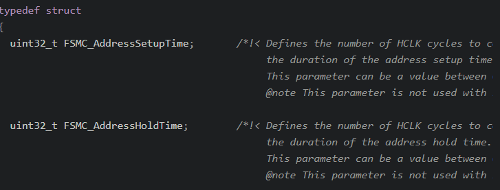
- typedef struct
- {
- uint32_t FSMC_AddressSetupTime; /*!< Defines the number of HCLK cycles to configure
- the duration of the address setup time.
- This parameter can be a value between 0 and 0xF.
- @note This parameter is not used with synchronous NOR Flash memories. */
- uint32_t FSMC_AddressHoldTime; /*!< Defines the number of HCLK cycles to configure
- the duration of the address hold time.
- This parameter can be a value between 0 and 0xF.
- @note This parameter is not used with synchronous NOR Flash memories.*/
- uint32_t FSMC_DataSetupTime; /*!< Defines the number of HCLK cycles to configure
- the duration of the data setup time.
- This parameter can be a value between 0 and 0xFF.
- @note This parameter is used for SRAMs, ROMs and asynchronous multiplexed NOR Flash memories. */
- uint32_t FSMC_BusTurnAroundDuration; /*!< Defines the number of HCLK cycles to configure
- the duration of the bus turnaround.
- This parameter can be a value between 0 and 0xF.
- @note This parameter is only used for multiplexed NOR Flash memories. */
- uint32_t FSMC_CLKDivision; /*!< Defines the period of CLK clock output signal, expressed in number of HCLK cycles.
- This parameter can be a value between 1 and 0xF.
- @note This parameter is not used for asynchronous NOR Flash, SRAM or ROM accesses. */
- uint32_t FSMC_DataLatency; /*!< Defines the number of memory clock cycles to issue
- to the memory before getting the first data.
- The parameter value depends on the memory type as shown below:
- - It must be set to 0 in case of a CRAM
- - It is don't care in asynchronous NOR, SRAM or ROM accesses
- - It may assume a value between 0 and 0xF in NOR Flash memories
- with synchronous burst mode enable */
- uint32_t FSMC_AccessMode; /*!< Specifies the asynchronous access mode.
- This parameter can be a value of @ref FSMC_Access_Mode */
- }FSMC_NORSRAMTimingInitTypeDef;
FSMC_NORSRAMInitTypeDef类型
- /**
- * @brief FSMC NOR/SRAM Init structure definition
- */
- typedef struct
- {
- uint32_t FSMC_Bank; /*!< Specifies the NOR/SRAM memory bank that will be used.
- This parameter can be a value of @ref FSMC_NORSRAM_Bank */
- uint32_t FSMC_DataAddressMux; /*!< Specifies whether the address and data values are
- multiplexed on the data bus or not.
- This parameter can be a value of @ref FSMC_Data_Address_Bus_Multiplexing */
- uint32_t FSMC_MemoryType; /*!< Specifies the type of external memory attached to
- the corresponding memory bank.
- This parameter can be a value of @ref FSMC_Memory_Type */
- uint32_t FSMC_MemoryDataWidth; /*!< Specifies the external memory device width.
- This parameter can be a value of @ref FSMC_Data_Width */
- uint32_t FSMC_BurstAccessMode; /*!< Enables or disables the burst access mode for Flash memory,
- valid only with synchronous burst Flash memories.
- This parameter can be a value of @ref FSMC_Burst_Access_Mode */
- uint32_t FSMC_AsynchronousWait; /*!< Enables or disables wait signal during asynchronous transfers,
- valid only with asynchronous Flash memories.
- This parameter can be a value of @ref FSMC_AsynchronousWait */
- uint32_t FSMC_WaitSignalPolarity; /*!< Specifies the wait signal polarity, valid only when accessing
- the Flash memory in burst mode.
- This parameter can be a value of @ref FSMC_Wait_Signal_Polarity */
- uint32_t FSMC_WrapMode; /*!< Enables or disables the Wrapped burst access mode for Flash
- memory, valid only when accessing Flash memories in burst mode.
- This parameter can be a value of @ref FSMC_Wrap_Mode */
- uint32_t FSMC_WaitSignalActive; /*!< Specifies if the wait signal is asserted by the memory one
- clock cycle before the wait state or during the wait state,
- valid only when accessing memories in burst mode.
- This parameter can be a value of @ref FSMC_Wait_Timing */
- uint32_t FSMC_WriteOperation; /*!< Enables or disables the write operation in the selected bank by the FSMC.
- This parameter can be a value of @ref FSMC_Write_Operation */
- uint32_t FSMC_WaitSignal; /*!< Enables or disables the wait state insertion via wait
- signal, valid for Flash memory access in burst mode.
- This parameter can be a value of @ref FSMC_Wait_Signal */
- uint32_t FSMC_ExtendedMode; /*!< Enables or disables the extended mode.
- This parameter can be a value of @ref FSMC_Extended_Mode */
- uint32_t FSMC_WriteBurst; /*!< Enables or disables the write burst operation.
- This parameter can be a value of @ref FSMC_Write_Burst */
- FSMC_NORSRAMTimingInitTypeDef* FSMC_ReadWriteTimingStruct; /*!< Timing Parameters for write and read access if the Extended Mode is not used*/
- FSMC_NORSRAMTimingInitTypeDef* FSMC_WriteTimingStruct; /*!< Timing Parameters for write access if the Extended Mode is used*/
- }FSMC_NORSRAMInitTypeDef;
FSMC_NAND_PCCARDTimingInitTypeDef类型
- /**
- * @brief Timing parameters For FSMC NAND and PCCARD Banks
- */
- typedef struct
- {
- uint32_t FSMC_SetupTime; /*!< Defines the number of HCLK cycles to setup address before
- the command assertion for NAND Flash read or write access
- to common/Attribute or I/O memory space (depending on
- the memory space timing to be configured).
- This parameter can be a value between 0 and 0xFF.*/
- uint32_t FSMC_WaitSetupTime; /*!< Defines the minimum number of HCLK cycles to assert the
- command for NAND Flash read or write access to
- common/Attribute or I/O memory space (depending on the
- memory space timing to be configured).
- This parameter can be a number between 0x00 and 0xFF */
- uint32_t FSMC_HoldSetupTime; /*!< Defines the number of HCLK clock cycles to hold address
- (and data for write access) after the command de-assertion
- for NAND Flash read or write access to common/Attribute
- or I/O memory space (depending on the memory space timing
- to be configured).
- This parameter can be a number between 0x00 and 0xFF */
- uint32_t FSMC_HiZSetupTime; /*!< Defines the number of HCLK clock cycles during which the
- data bus is kept in HiZ after the start of a NAND Flash
- write access to common/Attribute or I/O memory space (depending
- on the memory space timing to be configured).
- This parameter can be a number between 0x00 and 0xFF */
- }FSMC_NAND_PCCARDTimingInitTypeDef;
FSMC_NANDInitTypeDef类型
- /**
- * @brief FSMC NAND Init structure definition
- */
- typedef struct
- {
- uint32_t FSMC_Bank; /*!< Specifies the NAND memory bank that will be used.
- This parameter can be a value of @ref FSMC_NAND_Bank */
- uint32_t FSMC_Waitfeature; /*!< Enables or disables the Wait feature for the NAND Memory Bank.
- This parameter can be any value of @ref FSMC_Wait_feature */
- uint32_t FSMC_MemoryDataWidth; /*!< Specifies the external memory device width.
- This parameter can be any value of @ref FSMC_Data_Width */
- uint32_t FSMC_ECC; /*!< Enables or disables the ECC computation.
- This parameter can be any value of @ref FSMC_ECC */
- uint32_t FSMC_ECCPageSize; /*!< Defines the page size for the extended ECC.
- This parameter can be any value of @ref FSMC_ECC_Page_Size */
- uint32_t FSMC_TCLRSetupTime; /*!< Defines the number of HCLK cycles to configure the
- delay between CLE low and RE low.
- This parameter can be a value between 0 and 0xFF. */
- uint32_t FSMC_TARSetupTime; /*!< Defines the number of HCLK cycles to configure the
- delay between ALE low and RE low.
- This parameter can be a number between 0x0 and 0xFF */
- FSMC_NAND_PCCARDTimingInitTypeDef* FSMC_CommonSpaceTimingStruct; /*!< FSMC Common Space Timing */
- FSMC_NAND_PCCARDTimingInitTypeDef* FSMC_AttributeSpaceTimingStruct; /*!< FSMC Attribute Space Timing */
- }FSMC_NANDInitTypeDef;
FSMC_PCCARDInitTypeDef类型
- /**
- * @brief FSMC PCCARD Init structure definition
- */
- typedef struct
- {
- uint32_t FSMC_Waitfeature; /*!< Enables or disables the Wait feature for the Memory Bank.
- This parameter can be any value of @ref FSMC_Wait_feature */
- uint32_t FSMC_TCLRSetupTime; /*!< Defines the number of HCLK cycles to configure the
- delay between CLE low and RE low.
- This parameter can be a value between 0 and 0xFF. */
- uint32_t FSMC_TARSetupTime; /*!< Defines the number of HCLK cycles to configure the
- delay between ALE low and RE low.
- This parameter can be a number between 0x0 and 0xFF */
- FSMC_NAND_PCCARDTimingInitTypeDef* FSMC_CommonSpaceTimingStruct; /*!< FSMC Common Space Timing */
- FSMC_NAND_PCCARDTimingInitTypeDef* FSMC_AttributeSpaceTimingStruct; /*!< FSMC Attribute Space Timing */
- FSMC_NAND_PCCARDTimingInitTypeDef* FSMC_IOSpaceTimingStruct; /*!< FSMC IO Space Timing */
- }FSMC_PCCARDInitTypeDef;
相关宏定义
03. 相关函数
- /* NOR/SRAM Controller functions **********************************************/
- void FSMC_NORSRAMDeInit(uint32_t FSMC_Bank);
- void FSMC_NORSRAMInit(FSMC_NORSRAMInitTypeDef* FSMC_NORSRAMInitStruct);
- void FSMC_NORSRAMStructInit(FSMC_NORSRAMInitTypeDef* FSMC_NORSRAMInitStruct);
- void FSMC_NORSRAMCmd(uint32_t FSMC_Bank, FunctionalState NewState);
- /* NAND Controller functions **************************************************/
- void FSMC_NANDDeInit(uint32_t FSMC_Bank);
- void FSMC_NANDInit(FSMC_NANDInitTypeDef* FSMC_NANDInitStruct);
- void FSMC_NANDStructInit(FSMC_NANDInitTypeDef* FSMC_NANDInitStruct);
- void FSMC_NANDCmd(uint32_t FSMC_Bank, FunctionalState NewState);
- void FSMC_NANDECCCmd(uint32_t FSMC_Bank, FunctionalState NewState);
- uint32_t FSMC_GetECC(uint32_t FSMC_Bank);
- /* PCCARD Controller functions ************************************************/
- void FSMC_PCCARDDeInit(void);
- void FSMC_PCCARDInit(FSMC_PCCARDInitTypeDef* FSMC_PCCARDInitStruct);
- void FSMC_PCCARDStructInit(FSMC_PCCARDInitTypeDef* FSMC_PCCARDInitStruct);
- void FSMC_PCCARDCmd(FunctionalState NewState);
- /* Interrupts and flags management functions **********************************/
- void FSMC_ITConfig(uint32_t FSMC_Bank, uint32_t FSMC_IT, FunctionalState NewState);
- FlagStatus FSMC_GetFlagStatus(uint32_t FSMC_Bank, uint32_t FSMC_FLAG);
- void FSMC_ClearFlag(uint32_t FSMC_Bank, uint32_t FSMC_FLAG);
- ITStatus FSMC_GetITStatus(uint32_t FSMC_Bank, uint32_t FSMC_IT);
- void FSMC_ClearITPendingBit(uint32_t FSMC_Bank, uint32_t FSMC_IT);
04. 结构体封装
- typedef struct
- {
- __IO uint32_t BTCR[8]; /*!< NOR/PSRAM chip-select control register(BCR) and chip-select timing register(BTR), Address offset: 0x00-1C */
- } FSMC_Bank1_TypeDef;
- /**
- * @brief Flexible Static Memory Controller Bank1E
- */
- typedef struct
- {
- __IO uint32_t BWTR[7]; /*!< NOR/PSRAM write timing registers, Address offset: 0x104-0x11C */
- } FSMC_Bank1E_TypeDef;
- /**
- * @brief Flexible Static Memory Controller Bank2
- */
- typedef struct
- {
- __IO uint32_t PCR2; /*!< NAND Flash control register 2, Address offset: 0x60 */
- __IO uint32_t SR2; /*!< NAND Flash FIFO status and interrupt register 2, Address offset: 0x64 */
- __IO uint32_t PMEM2; /*!< NAND Flash Common memory space timing register 2, Address offset: 0x68 */
- __IO uint32_t PATT2; /*!< NAND Flash Attribute memory space timing register 2, Address offset: 0x6C */
- uint32_t RESERVED0; /*!< Reserved, 0x70 */
- __IO uint32_t ECCR2; /*!< NAND Flash ECC result registers 2, Address offset: 0x74 */
- } FSMC_Bank2_TypeDef;
- /**
- * @brief Flexible Static Memory Controller Bank3
- */
- typedef struct
- {
- __IO uint32_t PCR3; /*!< NAND Flash control register 3, Address offset: 0x80 */
- __IO uint32_t SR3; /*!< NAND Flash FIFO status and interrupt register 3, Address offset: 0x84 */
- __IO uint32_t PMEM3; /*!< NAND Flash Common memory space timing register 3, Address offset: 0x88 */
- __IO uint32_t PATT3; /*!< NAND Flash Attribute memory space timing register 3, Address offset: 0x8C */
- uint32_t RESERVED0; /*!< Reserved, 0x90 */
- __IO uint32_t ECCR3; /*!< NAND Flash ECC result registers 3, Address offset: 0x94 */
- } FSMC_Bank3_TypeDef;
- /**
- * @brief Flexible Static Memory Controller Bank4
- */
- typedef struct
- {
- __IO uint32_t PCR4; /*!< PC Card control register 4, Address offset: 0xA0 */
- __IO uint32_t SR4; /*!< PC Card FIFO status and interrupt register 4, Address offset: 0xA4 */
- __IO uint32_t PMEM4; /*!< PC Card Common memory space timing register 4, Address offset: 0xA8 */
- __IO uint32_t PATT4; /*!< PC Card Attribute memory space timing register 4, Address offset: 0xAC */
- __IO uint32_t PIO4; /*!< PC Card I/O space timing register 4, Address offset: 0xB0 */
- } FSMC_Bank4_TypeDef;
|
.png) STMCU小助手
发布时间:2022-3-29 09:52
STMCU小助手
发布时间:2022-3-29 09:52
 微信公众号
微信公众号
 手机版
手机版