01. 概述0 h; E$ S! ^; e0 `: k# q* \
FSMC 相关的库函数分布在 stm32f4xx_fsmc.c 文件和头文件 stm32f4xx_fsmc.h 中。- b4 N# b$ N% H3 F
% _5 g" c: M/ W( r' A- K* i# k02. 相关类型
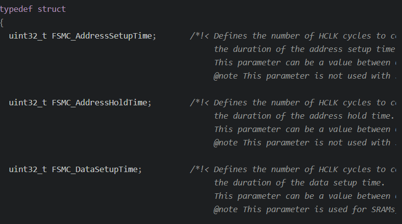
4 k9 V. f, e0 M$ u3 P0 X! yFSMC_NORSRAMTimingInitTypeDef类型7 y$ G& K$ L6 i& c4 k( R
5 J, o. j. |# O2 O1 }- 7 R( l8 E& R- I8 P7 w
- /** 9 n+ S# P3 `3 c1 J" t
- * @brief Timing parameters For NOR/SRAM Banks " P1 \' h% `' P' D+ a3 ?
- */" U/ `) {5 B4 {4 ]" b: N
- typedef struct& Q1 H. Z, Q) D, J) T& \3 k3 A* L: [
- {+ T) V: S% l4 {1 _5 x
- uint32_t FSMC_AddressSetupTime; /*!< Defines the number of HCLK cycles to configure$ R* a) X. ]9 U3 @
- the duration of the address setup time.
3 d) V) G5 r9 J' ?" o0 R9 d2 F - This parameter can be a value between 0 and 0xF.
4 x) A4 w( k3 v ] - @note This parameter is not used with synchronous NOR Flash memories. */% S2 Q) z, B# z9 Y# t7 m( {& J
- * F( H2 H; w u+ \/ X
- uint32_t FSMC_AddressHoldTime; /*!< Defines the number of HCLK cycles to configure3 ?. i5 |# X, r% O, T9 I
- the duration of the address hold time.7 u8 a! T8 G: D8 Q" Z8 K/ Q3 w
- This parameter can be a value between 0 and 0xF. 1 m! u9 }& r1 o; L5 \( b V( ~
- @note This parameter is not used with synchronous NOR Flash memories.*/2 x# z6 q6 T! N" r$ ^; @9 C8 y
- 6 ^6 M0 z! k3 |" E2 s
- uint32_t FSMC_DataSetupTime; /*!< Defines the number of HCLK cycles to configure
( V& m4 M7 J' I - the duration of the data setup time.7 P- \5 s: f+ N ^4 C3 O
- This parameter can be a value between 0 and 0xFF.( P0 c" b9 m; Z, P2 ^- F" J& t
- @note This parameter is used for SRAMs, ROMs and asynchronous multiplexed NOR Flash memories. *// G0 a, f& t* Y- s Z4 L
- 1 P/ L! l, Z( J5 X- o3 E+ p
- uint32_t FSMC_BusTurnAroundDuration; /*!< Defines the number of HCLK cycles to configure4 }! s- w- v0 T
- the duration of the bus turnaround.
' j: D4 Q( Z6 `! B - This parameter can be a value between 0 and 0xF.6 t' r( Y8 f0 t
- @note This parameter is only used for multiplexed NOR Flash memories. */2 v6 M' F4 M" ^6 ?: a9 `
3 ~- \, c, }( B. H9 n) f0 ?- uint32_t FSMC_CLKDivision; /*!< Defines the period of CLK clock output signal, expressed in number of HCLK cycles.7 r$ Q/ _$ h' A% \! G6 s! X
- This parameter can be a value between 1 and 0xF.6 o' e9 I$ e" Z6 O/ _- X
- @note This parameter is not used for asynchronous NOR Flash, SRAM or ROM accesses. */" |0 \. V6 N C V% u% l; e
- : E E5 T2 _7 A; |6 k1 g' s
- uint32_t FSMC_DataLatency; /*!< Defines the number of memory clock cycles to issue, Q: x' Q6 U9 {- O
- to the memory before getting the first data.8 p% f7 B v% @ U( v D+ e1 `5 E7 T
- The parameter value depends on the memory type as shown below:
- u/ w9 w+ B; H+ c% T& w% c - - It must be set to 0 in case of a CRAM3 Y: k7 \% V. e- a. u
- - It is don't care in asynchronous NOR, SRAM or ROM accesses
5 f, s" `) k2 y, E$ R+ Q - - It may assume a value between 0 and 0xF in NOR Flash memories9 z* z4 d% z( i- T- U4 G! Z
- with synchronous burst mode enable */
9 C! N2 r- x1 w: [3 c0 }1 V
1 U3 t% X- M. Y' G1 r' L5 H' y- uint32_t FSMC_AccessMode; /*!< Specifies the asynchronous access mode. ' i3 v _' z: |' U2 g e! t9 J2 { A
- This parameter can be a value of @ref FSMC_Access_Mode */+ Y% |, h7 g4 n+ ? `- l
- }FSMC_NORSRAMTimingInitTypeDef;
' ^* |- f. }0 Z( OFSMC_NORSRAMInitTypeDef类型
* h- g5 `% T9 R7 q! u! `
: y5 F% `" d$ d, j- /**
! Q. J3 l( ?+ ]. b, O) ]& {9 F - * @brief FSMC NOR/SRAM Init structure definition
+ n+ v* n/ u/ e- J; q/ [ \ - */
. F* P$ Q- u# k/ t7 T - typedef struct: p1 T8 |% Q, D% T( f
- {
; [3 z3 v* J) A3 }% D - uint32_t FSMC_Bank; /*!< Specifies the NOR/SRAM memory bank that will be used.
+ \# [/ _& _$ C6 r1 r. e - This parameter can be a value of @ref FSMC_NORSRAM_Bank */
+ K0 w& H+ u7 D4 b" o: b
' r3 K7 e2 e5 m0 k ^- uint32_t FSMC_DataAddressMux; /*!< Specifies whether the address and data values are" E+ r+ Y& p% @6 u# h
- multiplexed on the data bus or not.
! H/ w6 C5 J6 X, ~ - This parameter can be a value of @ref FSMC_Data_Address_Bus_Multiplexing */# X; h7 |; J7 J& `) v' {
- . ~+ q; x ~- v8 V
- uint32_t FSMC_MemoryType; /*!< Specifies the type of external memory attached to: H+ F. @" Q) M# K7 x6 n
- the corresponding memory bank.
9 u, q0 M& A* A5 J# S q - This parameter can be a value of @ref FSMC_Memory_Type */
# D$ c1 J! T- j. Q: O4 L2 d - / J- I1 X3 T8 _5 l( B& t7 X2 k/ b: P
- uint32_t FSMC_MemoryDataWidth; /*!< Specifies the external memory device width.
( m1 E. s! r: y+ @6 o, I - This parameter can be a value of @ref FSMC_Data_Width */
+ f+ B$ G, ]& u [$ X' X- s2 x1 [/ j
+ x4 P( t2 q( `: h- uint32_t FSMC_BurstAccessMode; /*!< Enables or disables the burst access mode for Flash memory,
& V$ y! `# f8 V* Z; E6 z - valid only with synchronous burst Flash memories.
- v: i& s @: b1 v7 Q. ? - This parameter can be a value of @ref FSMC_Burst_Access_Mode */
5 ~1 s6 t4 T2 b. q* ] - 2 P& y# F( U: C% M1 q. E
- uint32_t FSMC_AsynchronousWait; /*!< Enables or disables wait signal during asynchronous transfers,
* K& v1 B. U U/ q0 f+ b5 ~ - valid only with asynchronous Flash memories. |: U+ H+ }% b2 e& e
- This parameter can be a value of @ref FSMC_AsynchronousWait */ 2 q* O0 Q7 }2 M$ E3 d6 O
' W* U; H T5 V) c3 @; E! E( E- uint32_t FSMC_WaitSignalPolarity; /*!< Specifies the wait signal polarity, valid only when accessing2 R+ L) N& h+ Y$ J
- the Flash memory in burst mode.
9 ^4 ]0 K$ h g6 E9 r: Q - This parameter can be a value of @ref FSMC_Wait_Signal_Polarity */" z" B5 a* i4 d9 p
/ O2 n n- ^) {/ K$ B$ O. A: M- uint32_t FSMC_WrapMode; /*!< Enables or disables the Wrapped burst access mode for Flash* s' \* @* O5 w) F7 U$ g8 K
- memory, valid only when accessing Flash memories in burst mode.# u9 k# f! r: x" e3 ?
- This parameter can be a value of @ref FSMC_Wrap_Mode */2 T! @' t! g! _2 w# S/ Q
" H5 \% A& g+ S. H) V- uint32_t FSMC_WaitSignalActive; /*!< Specifies if the wait signal is asserted by the memory one) M8 t3 T& `' X& Q6 b, s
- clock cycle before the wait state or during the wait state,
" O+ u$ x! Z4 U% d$ g' j8 L# } - valid only when accessing memories in burst mode. " Y6 E8 |% [7 q7 O
- This parameter can be a value of @ref FSMC_Wait_Timing */
8 Z- S0 `+ l) ?0 N
+ y' }$ ~ ?; U. Z9 [* m& h' S- uint32_t FSMC_WriteOperation; /*!< Enables or disables the write operation in the selected bank by the FSMC.
J+ K* g" i0 a4 P- ?: t$ x4 [ - This parameter can be a value of @ref FSMC_Write_Operation */0 ^' w8 ?6 z6 j
- 0 z+ a& F- v5 ^* a) _
- uint32_t FSMC_WaitSignal; /*!< Enables or disables the wait state insertion via wait
' v2 e& I( f. n) F* `9 ? - signal, valid for Flash memory access in burst mode. G! ?; j6 ~$ ^( b! ~
- This parameter can be a value of @ref FSMC_Wait_Signal */
, W9 B" Z5 M) e; d6 v - * \5 M" |6 _7 C5 Y6 {! V: _
- uint32_t FSMC_ExtendedMode; /*!< Enables or disables the extended mode.
. r. o3 `9 r; o C6 C - This parameter can be a value of @ref FSMC_Extended_Mode */6 k3 Y1 L+ f8 |! Z/ x
. P& B) h4 r, x' M. e- ]- uint32_t FSMC_WriteBurst; /*!< Enables or disables the write burst operation.
7 W, C ^: n& `9 r" m - This parameter can be a value of @ref FSMC_Write_Burst */
$ s7 l1 p! q9 H6 z, f4 H* q) ?
- f3 G, ] o. g* T6 s- _- FSMC_NORSRAMTimingInitTypeDef* FSMC_ReadWriteTimingStruct; /*!< Timing Parameters for write and read access if the Extended Mode is not used*/
* ^& N7 @: l$ V! h1 K) M: n - + ]4 R3 W' V( Q+ `" R5 f% J4 `
- FSMC_NORSRAMTimingInitTypeDef* FSMC_WriteTimingStruct; /*!< Timing Parameters for write access if the Extended Mode is used*/
$ e, I; P7 \3 H - }FSMC_NORSRAMInitTypeDef;
FSMC_NAND_PCCARDTimingInitTypeDef类型& h: a/ A9 F1 } x% Y8 F
$ [) l* f) p4 N
- /** * w" N, X% n& ~) E9 T) Z& _3 ]- b% \
- * @brief Timing parameters For FSMC NAND and PCCARD Banks
8 {/ U3 s8 Y3 y k* z' L! _+ a - */& B1 Z8 \3 Y Q4 ]! q3 B7 G8 P
- typedef struct
- ^4 m% B3 A/ q" x4 c5 l - {1 L* U: @! E( \" R" a- X1 f1 z
- uint32_t FSMC_SetupTime; /*!< Defines the number of HCLK cycles to setup address before6 R3 J8 J* A: {
- the command assertion for NAND Flash read or write access% A$ L7 h% c4 L- R. k/ x
- to common/Attribute or I/O memory space (depending on
/ F) o' V7 D9 v& A5 M6 l" ~ - the memory space timing to be configured).
/ ^. d+ L+ r' q3 T) |( K - This parameter can be a value between 0 and 0xFF.*/- S: u; a; w( k' b; o. c5 _2 }
# k) F3 n# O) f1 ?# [- uint32_t FSMC_WaitSetupTime; /*!< Defines the minimum number of HCLK cycles to assert the
, L$ g$ |" p% b - command for NAND Flash read or write access to
& |; q6 Q+ p+ ^( U- P2 g - common/Attribute or I/O memory space (depending on the4 P' R% T, A2 x/ h' c6 X
- memory space timing to be configured). ' k. ]! n2 Y `& L; S
- This parameter can be a number between 0x00 and 0xFF */7 P ?- [" X/ F$ G" e9 |5 W* h
- a" G1 X8 J; ^. e: k% T/ } t
- uint32_t FSMC_HoldSetupTime; /*!< Defines the number of HCLK clock cycles to hold address4 q" t. j# S: W
- (and data for write access) after the command de-assertion, f9 Z) m0 z( c7 V( Z
- for NAND Flash read or write access to common/Attribute" I6 u0 a! |, C" _5 H
- or I/O memory space (depending on the memory space timing# V6 A0 l s! x$ p- @/ A. S
- to be configured).
- o7 X# r X; s* z5 { - This parameter can be a number between 0x00 and 0xFF */: s% j/ `- q3 n
- " [: l% `# K9 h0 v
- uint32_t FSMC_HiZSetupTime; /*!< Defines the number of HCLK clock cycles during which the
2 I* h4 }, Y: R) R- j2 z; v - data bus is kept in HiZ after the start of a NAND Flash
6 ^2 p- f7 \, J: } - write access to common/Attribute or I/O memory space (depending
3 W$ @9 a$ B+ `) r: m - on the memory space timing to be configured).
) x1 K7 M; B% r; A - This parameter can be a number between 0x00 and 0xFF */# T1 Z. H9 ?. _1 h
- }FSMC_NAND_PCCARDTimingInitTypeDef;
/ ^; t y( w& i9 uFSMC_NANDInitTypeDef类型
: \/ e' r6 o% E m, R6 _) F3 b: g
- /**
5 \9 E+ C9 v/ \( z4 |) ?. L - * @brief FSMC NAND Init structure definition
7 l/ S1 r4 o; v- D - */
, y% n* V, L" Y5 Y8 F# A - typedef struct
4 d6 S/ n2 L2 p. J - {3 s( z' \7 e8 ^3 {% p! }
- uint32_t FSMC_Bank; /*!< Specifies the NAND memory bank that will be used.
H! D6 z4 l+ ~& G) A: @ - This parameter can be a value of @ref FSMC_NAND_Bank */- q- }& } ~4 Q8 B3 I" ^
- 4 s: }' U& k, Q8 p; N5 M
- uint32_t FSMC_Waitfeature; /*!< Enables or disables the Wait feature for the NAND Memory Bank.
3 d2 s* n- a2 _1 G5 I - This parameter can be any value of @ref FSMC_Wait_feature */
+ m- O7 |1 T$ N4 D% \& x - ; [' a1 d' Y# j( `# x7 f
- uint32_t FSMC_MemoryDataWidth; /*!< Specifies the external memory device width.
: w- O; [: ~1 B" G$ I# p6 U - This parameter can be any value of @ref FSMC_Data_Width */& ]& d, R( v$ K6 z! ]7 s z
- 5 @0 [2 B; h4 S$ Y; v4 }; W" Y2 E
- uint32_t FSMC_ECC; /*!< Enables or disables the ECC computation.9 u- E$ m, k( ?
- This parameter can be any value of @ref FSMC_ECC */$ ~; x, m( l+ |6 H- D
- 1 i. {; ?1 _; M1 Y5 o n# ?
- uint32_t FSMC_ECCPageSize; /*!< Defines the page size for the extended ECC.' h/ u0 V0 U, M
- This parameter can be any value of @ref FSMC_ECC_Page_Size */8 k6 m# h& o' Y. ]5 T" F2 h: r
& F$ y5 d d, `3 c- uint32_t FSMC_TCLRSetupTime; /*!< Defines the number of HCLK cycles to configure the
' q" w R, C( }1 _+ O: _ - delay between CLE low and RE low.
/ h: \! U4 M1 D2 I3 m! {9 O - This parameter can be a value between 0 and 0xFF. */, a; L- P4 ?) J" W
- : B: P3 w! ]1 N W' a) n+ m! q
- uint32_t FSMC_TARSetupTime; /*!< Defines the number of HCLK cycles to configure the
3 Q- l9 E8 d3 ]0 H - delay between ALE low and RE low.7 C4 Q+ b) ?( P5 g4 @
- This parameter can be a number between 0x0 and 0xFF */ 2 U, H6 k4 O3 E3 Q ~
- 3 o- ^% N. h2 `1 x, V+ i) m
- FSMC_NAND_PCCARDTimingInitTypeDef* FSMC_CommonSpaceTimingStruct; /*!< FSMC Common Space Timing */ / T. g/ U8 Z6 j3 J+ T4 y
7 p) [# m; e: h( ^8 ~- FSMC_NAND_PCCARDTimingInitTypeDef* FSMC_AttributeSpaceTimingStruct; /*!< FSMC Attribute Space Timing */3 C+ B; a0 C6 z9 d( h. X
- }FSMC_NANDInitTypeDef;
4 A& c$ {% P! A! vFSMC_PCCARDInitTypeDef类型( h; t" H+ Q6 a* U
: y- [) _1 D; z5 b. Q8 `5 G8 ^: n- /**
7 @) l5 N1 z: F; x4 w L& h - * @brief FSMC PCCARD Init structure definition
& z! @) @6 w) K1 J - */
3 O* {: z* g2 g0 P
' t1 e1 r- K0 w% a- typedef struct: u9 o3 @0 x2 f* O( v- |# M. X9 ]
- {! L2 `5 A& `4 v
- uint32_t FSMC_Waitfeature; /*!< Enables or disables the Wait feature for the Memory Bank.' n: a' b: U7 e2 s. \
- This parameter can be any value of @ref FSMC_Wait_feature */
( k: H/ J; E5 I5 V
v; z; f* o: ?" {0 t! L+ w- uint32_t FSMC_TCLRSetupTime; /*!< Defines the number of HCLK cycles to configure the% D6 V9 L0 c" t; @9 H7 }
- delay between CLE low and RE low. |; v& V/ d" {% F# f1 M
- This parameter can be a value between 0 and 0xFF. */
3 C9 ^2 Z) w' w
' ?# ^8 s9 p' O: c' ^6 E4 f- uint32_t FSMC_TARSetupTime; /*!< Defines the number of HCLK cycles to configure the8 d$ X i6 L: h
- delay between ALE low and RE low.
5 ^( u" S& A0 `8 Y - This parameter can be a number between 0x0 and 0xFF */ 7 L& A/ [& C" d/ g8 `7 Y
- , c1 j8 F1 h4 k* G2 U
2 D0 d* i& [9 w! W- FSMC_NAND_PCCARDTimingInitTypeDef* FSMC_CommonSpaceTimingStruct; /*!< FSMC Common Space Timing */
. k! C z( n6 `' `0 O - 5 r# |2 |* S0 r! E& E: E$ U
- FSMC_NAND_PCCARDTimingInitTypeDef* FSMC_AttributeSpaceTimingStruct; /*!< FSMC Attribute Space Timing */
- x( G2 O& r( I) @7 b - 0 x( D# i" J3 }; n
- FSMC_NAND_PCCARDTimingInitTypeDef* FSMC_IOSpaceTimingStruct; /*!< FSMC IO Space Timing */ - B+ x; q& T. ?' S3 X9 L
- }FSMC_PCCARDInitTypeDef;
相关宏定义
) } h, Z m" }2 h- g2 l v- a$ }
{+ K7 j9 p9 z6 {$ o* E- /** @defgroup FSMC_Exported_Constants" p, f# ?4 @$ Y9 Z3 o
- * @{6 X* W6 v6 d" e3 B. P& G
- */
1 R2 {' i% n+ Y% r - 8 w! D' g7 K2 D# d! W
- /** @defgroup FSMC_NORSRAM_Bank
" @% I( X6 K% S) W' @ - * @{
. Q0 d' q! X. g/ c2 @8 _9 ~# q& Y - */+ Q( v) @1 G: z, h g3 b" q
- #define FSMC_Bank1_NORSRAM1 ((uint32_t)0x00000000)
% O; c( C5 H& J% n - #define FSMC_Bank1_NORSRAM2 ((uint32_t)0x00000002)
- L' Z% f% K6 a# f - #define FSMC_Bank1_NORSRAM3 ((uint32_t)0x00000004)5 j% z- x; E1 ~" m. W
- #define FSMC_Bank1_NORSRAM4 ((uint32_t)0x00000006) W B6 b# {# L2 b' H# H
- /**
' u3 y- _' C) b1 |9 F7 ] - * @}$ \1 e- e% P6 `! F5 _9 ?7 X/ F
- */
0 k0 J" W9 t9 b4 `5 J+ p0 M. H
4 Y/ M) T1 [8 Q! K- /** @defgroup FSMC_NAND_Bank
& T( z7 G* ~& c" T* ?) H - * @{- U) J9 n e4 S
- */
/ }5 \) ? i% o* T2 O3 j - #define FSMC_Bank2_NAND ((uint32_t)0x00000010)
# F3 }+ v8 a+ H N - #define FSMC_Bank3_NAND ((uint32_t)0x00000100)' ~; u+ A: D! d$ N8 P! x
- /**
D6 S5 u6 C8 ~' R, Q8 c - * @}
" k3 H' ]2 J; K& D( I- D+ ` - */
$ s) N/ h5 v' G, i2 @' z3 _% v - + q3 T; Q5 [* b2 b# Q7 ]
- /** @defgroup FSMC_PCCARD_Bank
' Y" ?* h2 {; X4 ` - * @{
; u! h9 Y1 U2 F) X - */
+ B: A4 O0 K! T" y - #define FSMC_Bank4_PCCARD ((uint32_t)0x00001000)8 Z2 ]& Y k; ^6 i/ n* d7 T
- /**! j& M! c1 `( z" ?; q) X, J
- * @}4 H. Z/ M; |' J! a$ D: N+ [6 y
- */
: J, Z1 r( T6 }: o9 P9 F" c
7 X! `8 z5 K2 L( l4 K( U8 e3 X; o- #define IS_FSMC_NORSRAM_BANK(BANK) (((BANK) == FSMC_Bank1_NORSRAM1) || \. U( N5 Z g( U, M5 h; n
- ((BANK) == FSMC_Bank1_NORSRAM2) || \( ?8 I) w; \/ C- z( z% y
- ((BANK) == FSMC_Bank1_NORSRAM3) || \. G% `1 H6 n) q+ c0 l$ ~9 ^
- ((BANK) == FSMC_Bank1_NORSRAM4))
. \5 u5 ?; P* ?. N" ~ - # Q- Z2 ~$ j7 q0 V( s) ]9 p' q$ ]
- #define IS_FSMC_NAND_BANK(BANK) (((BANK) == FSMC_Bank2_NAND) || \5 S9 T E% }) W/ U5 w5 ^- a
- ((BANK) == FSMC_Bank3_NAND))2 _" [& ]% {7 n$ h7 e- j k
/ m0 u% X! Z6 ^6 R3 k n- #define IS_FSMC_GETFLAG_BANK(BANK) (((BANK) == FSMC_Bank2_NAND) || \
& V2 m! S- V- N - ((BANK) == FSMC_Bank3_NAND) || \
- T! Z$ k7 w4 E& M1 I' u7 x - ((BANK) == FSMC_Bank4_PCCARD))9 Q/ P. I/ t) E$ e$ }' p
# F4 S9 Q0 q* o7 u$ L* X. A7 n- #define IS_FSMC_IT_BANK(BANK) (((BANK) == FSMC_Bank2_NAND) || \
0 b7 \7 C; d) Y - ((BANK) == FSMC_Bank3_NAND) || \
9 T; p( b( R$ i$ J, S H8 `, J - ((BANK) == FSMC_Bank4_PCCARD))% Y0 E6 K- j, y6 G
# z/ o/ T: {; v) E- /** @defgroup FSMC_NOR_SRAM_Controller 2 ?) b4 ^1 }. b8 c
- * @{" P5 t |7 n: i9 J7 `
- */- s1 n; S, z9 p
0 O) A8 N2 K+ K* d' O# I- /** @defgroup FSMC_Data_Address_Bus_Multiplexing
( Z) _4 K6 D# R: s" ^7 d* J m( e& G - * @{
7 i* N8 q1 J# u+ w6 X& P - */1 C) J& Q7 y L5 Z
c, @' ?8 ]4 g+ \3 I- #define FSMC_DataAddressMux_Disable ((uint32_t)0x00000000)
+ V. y6 O6 \ g# _1 }; Z& e5 P - #define FSMC_DataAddressMux_Enable ((uint32_t)0x00000002)
( ~: h' k3 h9 @; Q' j - #define IS_FSMC_MUX(MUX) (((MUX) == FSMC_DataAddressMux_Disable) || \
9 @" \. R9 Y& u* P. Y: F - ((MUX) == FSMC_DataAddressMux_Enable))+ O$ V: Z e( l' z8 h$ m$ s' u3 r
- /**
2 F: V3 A: V" h# a7 K$ l$ D$ l2 x9 y - * @}
, T9 Z0 R: [) \ - */8 Y x; t+ {+ I% O; p3 m: ^, [ f
; H6 S3 N, i, W" D% ]* {- /** @defgroup FSMC_Memory_Type
0 D q8 u, C6 i3 m3 K0 d - * @{
2 m# J- i4 {9 V6 P L" t; E Y) S - */
& L }, z5 |0 |4 n" X2 J
; p7 V; b# j3 D0 O" s- #define FSMC_MemoryType_SRAM ((uint32_t)0x00000000)0 ]& c% \3 q+ N" M# c, E! i
- #define FSMC_MemoryType_PSRAM ((uint32_t)0x00000004)
* Y4 l9 ~4 Y! `: V - #define FSMC_MemoryType_NOR ((uint32_t)0x00000008)
4 Y/ q7 R" s! x& h1 |' t; a - #define IS_FSMC_MEMORY(MEMORY) (((MEMORY) == FSMC_MemoryType_SRAM) || \2 Z6 h, T) I% Z6 X% c; A
- ((MEMORY) == FSMC_MemoryType_PSRAM)|| \' n6 ~$ R: _" e2 Z0 @( u% X1 F
- ((MEMORY) == FSMC_MemoryType_NOR))( _: W+ u. w& m' a0 A4 t$ S
- /**" ^ R S, W# P% \. [" K" J! Y
- * @}
- Q6 F4 N E% Y, ?8 m - */# J% K6 K& x, C# I9 s
- e3 ^; f* G- ]5 C4 i7 v- /** @defgroup FSMC_Data_Width & r7 t4 L! L% m! l; ~0 R* w
- * @{6 ~( i( U9 f( w& k; u
- */# ?8 c, W# _* T* f& {
$ D2 F$ l8 ^" `- #define FSMC_MemoryDataWidth_8b ((uint32_t)0x00000000)2 D, w: Q$ l; c
- #define FSMC_MemoryDataWidth_16b ((uint32_t)0x00000010)
/ K) a% w& L6 T6 l$ J - #define IS_FSMC_MEMORY_WIDTH(WIDTH) (((WIDTH) == FSMC_MemoryDataWidth_8b) || \
# k/ l7 X v. c, V, R3 L - ((WIDTH) == FSMC_MemoryDataWidth_16b))
X! N' G3 G2 b9 I/ s$ Z! H - /**) }/ O& w, z: c# B' v+ j" g
- * @}) \# U7 U: q7 T
- */
$ S) s7 X. m& @3 q: w - 6 V, _6 K- i) q. Q* g
- /** @defgroup FSMC_Burst_Access_Mode
) M' m0 E e( @5 O2 S: d - * @{: k9 p; V ]& A* E+ x
- */
. ~! K) b6 Q; a3 q - 5 W) Q& C! q; [/ E2 p/ d7 V4 n0 E
- #define FSMC_BurstAccessMode_Disable ((uint32_t)0x00000000)
+ N- x$ h: U& m9 \7 d4 ~6 O* c& U& I - #define FSMC_BurstAccessMode_Enable ((uint32_t)0x00000100)
$ I1 f$ D4 I ]3 C1 k0 M - #define IS_FSMC_BURSTMODE(STATE) (((STATE) == FSMC_BurstAccessMode_Disable) || \) G, C7 D; f8 e
- ((STATE) == FSMC_BurstAccessMode_Enable))( c7 T4 T* j" i; I3 F& w( k
- /**
- `' u# p: s+ u% T - * @}! C$ F- g: } I" ~2 g
- */
7 y# a- r) j* b5 v$ S0 ^: V
1 p$ h& W S+ Q. X- /** @defgroup FSMC_AsynchronousWait 2 S( j0 o. D4 i# c9 D1 M+ Y! i+ N
- * @{" c! P+ ]8 s( _ `
- */
! x* P. d5 D0 ?/ U6 n2 ^# u - #define FSMC_AsynchronousWait_Disable ((uint32_t)0x00000000); [% H( a5 M& E3 _5 s U9 Q
- #define FSMC_AsynchronousWait_Enable ((uint32_t)0x00008000)% ^/ H2 Q1 n7 g2 N- _
- #define IS_FSMC_ASYNWAIT(STATE) (((STATE) == FSMC_AsynchronousWait_Disable) || \9 p: j& L4 W+ T3 r* X0 x
- ((STATE) == FSMC_AsynchronousWait_Enable))
9 f( m- ^. _ J5 x - /**) l! K; c" f; u3 b
- * @}
9 H. X6 i# s7 g; K, ] - */6 e7 _, t3 r; I# V& e
% p$ w2 A% t: G& u; P' T- /** @defgroup FSMC_Wait_Signal_Polarity
% s) {6 [( `5 B - * @{% W: n$ S7 P2 P* C" Q
- */
% i7 {$ @$ d# s( W' Q - #define FSMC_WaitSignalPolarity_Low ((uint32_t)0x00000000)
B, Y- z& {0 U, J) J( z- Z0 w - #define FSMC_WaitSignalPolarity_High ((uint32_t)0x00000200)
1 Q8 p3 Z3 K7 V- R- y - #define IS_FSMC_WAIT_POLARITY(POLARITY) (((POLARITY) == FSMC_WaitSignalPolarity_Low) || \
- ]6 H! p' c2 K$ i6 l$ f2 p - ((POLARITY) == FSMC_WaitSignalPolarity_High))
6 z! F, E7 {6 w, k - /**
; b$ y, w, H: U9 e# ~8 P - * @}
2 U) S) g3 }- F" c* n - */" g& S3 m4 P# A* t
. s2 B# ~" x$ o- /** @defgroup FSMC_Wrap_Mode ; R {" p0 j2 {1 w# R9 [. M
- * @{
& D1 ~2 j- J& o5 B3 i0 u - */! z2 N& o& Z, R% e# f
- #define FSMC_WrapMode_Disable ((uint32_t)0x00000000) d3 i" k, P( H( Z1 P+ l) g: L
- #define FSMC_WrapMode_Enable ((uint32_t)0x00000400)
Y" b0 C7 Y/ N4 [9 t& Y; A# M - #define IS_FSMC_WRAP_MODE(MODE) (((MODE) == FSMC_WrapMode_Disable) || \$ H$ y( A( G( y6 W# i
- ((MODE) == FSMC_WrapMode_Enable))& V9 Y C0 }) w
- /**5 N3 G1 }; z$ \7 [
- * @}. W$ V4 z2 i8 g7 }8 E9 B
- */
& M2 [$ K' }/ b/ t: r! k
/ A# W: T$ Q0 Y6 d$ Y3 n7 F: m N. u- /** @defgroup FSMC_Wait_Timing ! }* t" F. z }! w
- * @{
9 T3 l1 Y$ x6 _ - */0 t4 a' T* t" ~ W) u
- #define FSMC_WaitSignalActive_BeforeWaitState ((uint32_t)0x00000000)
) M6 Z/ I8 s% | - #define FSMC_WaitSignalActive_DuringWaitState ((uint32_t)0x00000800) 7 K% O) H# s- b9 M5 ]
- #define IS_FSMC_WAIT_SIGNAL_ACTIVE(ACTIVE) (((ACTIVE) == FSMC_WaitSignalActive_BeforeWaitState) || \
1 l/ o. M G7 O/ _* G$ s' W6 a - ((ACTIVE) == FSMC_WaitSignalActive_DuringWaitState))
9 N4 E& N6 h6 {9 k+ n - /**
5 `, x6 q9 _6 J" |1 }/ f - * @}
# t% R% I; ]6 C$ e% y - */6 p! O' M3 y0 `2 r: S5 x) K
! @4 C4 T9 O: ?5 C8 @3 j- /** @defgroup FSMC_Write_Operation . X4 d/ m% r6 ~/ S K* \ e
- * @{
9 l- G5 ]0 z2 @. v* o& i - */# q }- L* S0 ~
- #define FSMC_WriteOperation_Disable ((uint32_t)0x00000000)
% _. l0 J, ?; g! d# ~3 o% C& Q - #define FSMC_WriteOperation_Enable ((uint32_t)0x00001000)9 ^+ g' g! S" W% P' |
- #define IS_FSMC_WRITE_OPERATION(OPERATION) (((OPERATION) == FSMC_WriteOperation_Disable) || \
+ n* h/ W5 {" L3 s# i' E - ((OPERATION) == FSMC_WriteOperation_Enable)) 3 N' \" b) e/ @
- /**
" ]/ d" M8 j+ t/ `/ B - * @}- g& p/ [! Y& ~3 _2 Q% h! i
- */
. E- o7 H. b* b3 h: g - " f, f7 O0 ]1 E4 V; U
- /** @defgroup FSMC_Wait_Signal
' a5 k" c' a7 `/ ?2 O7 \ - * @{
2 ^4 X5 A% J, H* F6 y( `7 v" e - */) W3 k2 `) l* {* g& o2 y
- #define FSMC_WaitSignal_Disable ((uint32_t)0x00000000)
9 ^" I$ {; U' b: A# k. c - #define FSMC_WaitSignal_Enable ((uint32_t)0x00002000) ! k9 @" Y" X \+ a
- #define IS_FSMC_WAITE_SIGNAL(SIGNAL) (((SIGNAL) == FSMC_WaitSignal_Disable) || \
: A9 N4 c+ Q3 W& { - ((SIGNAL) == FSMC_WaitSignal_Enable))2 t$ J1 f3 ]+ G6 z% |* ]
- /**5 S$ n; b F2 V$ P! M& p! u
- * @}
7 x" u# X4 z$ V5 { - */
8 h2 W* x. j6 g - ' V: p* y, t& h, P) q5 @) m' U
- /** @defgroup FSMC_Extended_Mode 5 D# j5 y y% V3 t. S
- * @{
5 J/ z+ e1 ~3 @5 Y; U - */; b6 ^) p. A: d, y0 p# a8 j% ?
- #define FSMC_ExtendedMode_Disable ((uint32_t)0x00000000)
' k0 I& _9 y6 m/ f" I - #define FSMC_ExtendedMode_Enable ((uint32_t)0x00004000)
1 H7 i) T X8 J8 u& H
$ P! E# u3 E$ M0 N" A- #define IS_FSMC_EXTENDED_MODE(MODE) (((MODE) == FSMC_ExtendedMode_Disable) || \7 G; n0 r! `" [: v/ C) x
- ((MODE) == FSMC_ExtendedMode_Enable)) 1 G. \/ u& ?6 Q4 R* S% p
- /**8 X2 o8 _4 [! x) b& x; j3 n
- * @}
" M2 j" S) Q' r, |& ] - */, o6 t- o4 v3 m- ^# [
- Z- ?* z w( C7 X1 n
- /** @defgroup FSMC_Write_Burst 4 e# r7 Z$ w1 N. s1 u2 {( x
- * @{7 h5 n4 }* K& {/ n+ t& t" f
- */ C8 W) F1 R$ t
. I, h- G; j* r( [- #define FSMC_WriteBurst_Disable ((uint32_t)0x00000000)
2 I; w W! W& _6 k - #define FSMC_WriteBurst_Enable ((uint32_t)0x00080000) ; |2 j; u2 T; |! A& ^
- #define IS_FSMC_WRITE_BURST(BURST) (((BURST) == FSMC_WriteBurst_Disable) || \- H8 h# Y9 Y6 \2 @# u# T0 E
- ((BURST) == FSMC_WriteBurst_Enable))3 ~* Y4 o: u) w9 X7 |& `6 J. u
- /**! \0 f+ @" l# S; o# `/ g8 u! I
- * @}
j9 [, J0 @9 D; P2 c1 n( w - */
. N e6 P( K! x1 O/ z6 A
/ g S# e( u' D. b% L- /** @defgroup FSMC_Address_Setup_Time
; u- N, g r7 K6 e q - * @{
" k% C. A# P2 a% `9 t' w - */* t, Y9 x7 U; Z7 w! ?. {
- #define IS_FSMC_ADDRESS_SETUP_TIME(TIME) ((TIME) <= 0xF): ~, l' y% L/ I& W
- /**% w. y4 L* ~- Q3 }! u; d/ g: |7 g$ q& d
- * @}) H7 i2 H" Q1 {! n: y
- */' }; {5 W' J' @3 S* Z
- * u! [, C8 x9 }0 j$ u
- /** @defgroup FSMC_Address_Hold_Time : k4 f; U# M: L8 N1 K; e
- * @{" V4 b7 a9 [1 _3 _2 l7 m5 u
- */0 o! m1 @% z0 v+ ]
- #define IS_FSMC_ADDRESS_HOLD_TIME(TIME) ((TIME) <= 0xF)% j/ u' q6 n) x
- /**$ h% M2 ]2 D3 t' h( G0 {
- * @} q0 h% t5 j8 [ [- I: m
- */
0 Q. \$ V) v" g" |
1 t8 @) D. p' [4 l% d- /** @defgroup FSMC_Data_Setup_Time 7 |( X. O0 f) o/ x' N7 E; D2 l. J
- * @{
7 u' A9 f. z) n& f" k5 T2 K; E, X' i - */( g( ?9 M! B$ M2 p. ]
- #define IS_FSMC_DATASETUP_TIME(TIME) (((TIME) > 0) && ((TIME) <= 0xFF))
6 t$ S! M) X% i) N - /**! y1 T& @" ^% l. z
- * @}
' Q) e* E' k; q A' X! t9 w( @4 c - */
8 j0 k' K- T) Q4 Y
9 ?3 G6 t* Q- ]; j! a- /** @defgroup FSMC_Bus_Turn_around_Duration
0 }; b% h4 J2 w5 C' g! ^ - * @{
/ f5 z1 I2 K1 L# m) \; J- q w: ? - */
+ d0 ?: O2 F) G- k8 @, T - #define IS_FSMC_TURNAROUND_TIME(TIME) ((TIME) <= 0xF)% |2 ]4 @2 E* u4 K; ]1 ~9 s
- /**! ?# p( w B& z3 ]
- * @}# D; ]" Q H3 r
- *// u% c/ W- M2 P1 l
* m* T! f" }5 m5 @0 K8 I! d- /** @defgroup FSMC_CLK_Division
. o5 ^% s# c; M0 L; z6 s" ? - * @{8 z9 A" [. d# A# {
- */9 b8 {, G6 b/ i6 Y
- #define IS_FSMC_CLK_DIV(DIV) ((DIV) <= 0xF)
# n, C; y% g" U9 O# D/ _& Z - /**& M- b/ N: Z1 d! K# k$ p( @, E
- * @}. l' D" a- [8 L' v/ W
- */ B t: T# {5 @& ^3 E
- $ z7 [7 k& C q* ]! R
- /** @defgroup FSMC_Data_Latency # ^! ^7 i2 z. @9 {
- * @{4 T' `0 _% M9 }6 a# I
- */
% o7 D; w3 D2 g; |) u7 D - #define IS_FSMC_DATA_LATENCY(LATENCY) ((LATENCY) <= 0xF)6 a* Q! T4 p& N: j2 [0 r
- /**# V4 r" R1 O. t0 R# [3 N) n: j
- * @}
! t5 z2 q+ f& K3 r. U) C: Y; z - */
* Z# ]" x+ ~2 t7 {* O1 N) j
0 q4 A5 u' e2 J9 T4 _! L: s1 V- /** @defgroup FSMC_Access_Mode
# R. x8 S$ V7 [ t - * @{
* H; G& z$ ?/ f/ r5 n. Z% s - */* m9 S: N) B5 ?8 j( d, F6 }& y
- #define FSMC_AccessMode_A ((uint32_t)0x00000000)7 E* i( ]+ I2 o# b" k5 x
- #define FSMC_AccessMode_B ((uint32_t)0x10000000)
, C* D( _8 q1 M - #define FSMC_AccessMode_C ((uint32_t)0x20000000)
! M3 X S# Z) |1 q - #define FSMC_AccessMode_D ((uint32_t)0x30000000)
* a, ^: a. w9 l* ~5 g- ]. K - #define IS_FSMC_ACCESS_MODE(MODE) (((MODE) == FSMC_AccessMode_A) || \
$ a) ]" q; a" k6 b$ F T4 E - ((MODE) == FSMC_AccessMode_B) || \
1 e0 x2 _1 L9 e- C2 o- R8 e* w - ((MODE) == FSMC_AccessMode_C) || \, k7 g; Y* Z6 \( Q. S* b; |
- ((MODE) == FSMC_AccessMode_D))) z$ v8 w5 D6 D3 X! k0 F6 \( u
- /**
. Z# u) h7 _# j+ L2 F$ D+ Z - * @}
" e& v; l( k5 b! c - */( K+ F! y$ H% [, D( K& ?
- ' E3 }' {0 @) W R, X# ?
- /**. M3 d% Y9 I: B/ H! Z; @7 \% K
- * @}
4 a1 M) v/ _, m1 {& N8 @8 _' ? - */3 ?8 o( i2 ^% Z: M7 Z7 _8 L. @) O
' F( D4 `( i' q- /** @defgroup FSMC_NAND_PCCARD_Controller ' G9 G7 V8 i2 O" V# `* b
- * @{
& F K# Y0 B& G, o! r6 q$ F- ~( ~) r - */8 \5 f" V0 W& W9 K) o/ U
- , H9 W) M. n4 S Q% u3 |7 S
- /** @defgroup FSMC_Wait_feature ; z5 B& l( ]/ _0 U# j" P& `2 S
- * @{8 {8 d) l. [9 p" n2 }
- */
1 q# N- T0 ]+ d3 v0 z+ h# j' U6 I - #define FSMC_Waitfeature_Disable ((uint32_t)0x00000000). x; i& T+ j7 `% Q
- #define FSMC_Waitfeature_Enable ((uint32_t)0x00000002)2 [, W0 W8 v, F. U4 }' g- c
- #define IS_FSMC_WAIT_FEATURE(FEATURE) (((FEATURE) == FSMC_Waitfeature_Disable) || \! S3 h. O* D, i! a. Q% t# r c# L
- ((FEATURE) == FSMC_Waitfeature_Enable))$ Z% t$ ]1 l6 C0 z* i( x! T% e/ J
- /**
* H0 _5 Q, j5 Q0 s( m - * @}9 z1 j7 Z! |3 Q, r# k5 ~) s, r& i* b
- */
8 k1 C1 j! @. z - ! Q) T1 U/ ]; y9 o- @( z- o9 @; A
4 N! H/ p) n) n+ W- /** @defgroup FSMC_ECC
& w* V4 e4 Z* U# q, i - * @{. R9 W f2 w R8 c" c3 j' x
- */
% H3 B m$ ~4 f0 e - #define FSMC_ECC_Disable ((uint32_t)0x00000000)
! N$ q: i' u2 \: s% a9 G - #define FSMC_ECC_Enable ((uint32_t)0x00000040)
5 Z n/ f5 @* a4 t6 t - #define IS_FSMC_ECC_STATE(STATE) (((STATE) == FSMC_ECC_Disable) || \
! b6 a, @6 b- i K1 h" N4 \ - ((STATE) == FSMC_ECC_Enable))
# v/ l: [+ |5 j8 K; V: N/ O! V/ R - /**
2 G X$ |- F4 E1 H - * @}! b0 V H* j( ?& V5 @9 \1 k
- */
# q2 \" J) L% j0 Q* e3 P - 2 u2 ?) L# k$ I2 w% l" a* S
- /** @defgroup FSMC_ECC_Page_Size
! y! z) G% h4 t( w - * @{8 n! Q O0 h. I8 I) A
- */0 i, l, M. f; s
- #define FSMC_ECCPageSize_256Bytes ((uint32_t)0x00000000): w, f6 _8 }" ~4 b8 F1 b5 c
- #define FSMC_ECCPageSize_512Bytes ((uint32_t)0x00020000)7 H( \5 g7 i6 m% Y" J0 k
- #define FSMC_ECCPageSize_1024Bytes ((uint32_t)0x00040000)
" `1 K) v: X, L8 { - #define FSMC_ECCPageSize_2048Bytes ((uint32_t)0x00060000)2 l9 W3 O* c" E2 l2 l
- #define FSMC_ECCPageSize_4096Bytes ((uint32_t)0x00080000)6 V5 R+ J$ W8 c4 Y8 `
- #define FSMC_ECCPageSize_8192Bytes ((uint32_t)0x000A0000)
2 M% f0 N: Z- b% u6 {( ` - #define IS_FSMC_ECCPAGE_SIZE(SIZE) (((SIZE) == FSMC_ECCPageSize_256Bytes) || \4 p4 Z0 J$ y* e+ I$ G1 J
- ((SIZE) == FSMC_ECCPageSize_512Bytes) || \
7 K5 J7 v }9 ?3 A9 m; G - ((SIZE) == FSMC_ECCPageSize_1024Bytes) || \# ^! ~. P3 ^1 g2 K0 @
- ((SIZE) == FSMC_ECCPageSize_2048Bytes) || \/ O* n9 g: P: S. p
- ((SIZE) == FSMC_ECCPageSize_4096Bytes) || \
1 r& l& ^% h/ ~! L% u - ((SIZE) == FSMC_ECCPageSize_8192Bytes))) n0 I- ^* L" W$ |6 B9 B/ ^
- /**
3 Z- ~7 r- b$ k# u) a6 u/ I! t% t - * @}, A# T: ^# s. g! l
- */
) u7 Y" M4 u% C5 W# u% E - 5 I! o- g& P, O# Z$ u4 A" k' B
- /** @defgroup FSMC_TCLR_Setup_Time
- v, I5 G V) x0 H% d8 q - * @{
' J" y1 p. \% Q" w8 I' Q - */
g; ~% w: b# n# s - #define IS_FSMC_TCLR_TIME(TIME) ((TIME) <= 0xFF)
" e! `/ d `5 U0 D - /**; o7 ` g+ {' n0 x5 E5 U* m
- * @}, u( y& D4 I1 z& T: I
- */
2 s6 V" r3 O; Q
+ G5 Y% v$ R* c. q- /** @defgroup FSMC_TAR_Setup_Time " l4 }& p0 D& a( I, t) N
- * @{) m/ P: W- j5 W, ~
- */8 M% d5 W; z, ~. q1 n
- #define IS_FSMC_TAR_TIME(TIME) ((TIME) <= 0xFF)
) y& u9 s7 t/ A( g" d3 F - /**- Q" T7 M5 x7 x1 n2 W0 H% q9 Y
- * @}
/ k. w2 G- o. X8 |) D6 J - */
2 {& `/ ^+ F, y- _/ P: W o7 K! x7 x
D. Z* o/ q( \5 S) o' X- /** @defgroup FSMC_Setup_Time 9 S+ |; Z3 S3 I5 {
- * @{6 ~1 g. X# A P9 D2 y
- */
4 \1 h! x! }# k - #define IS_FSMC_SETUP_TIME(TIME) ((TIME) <= 0xFF)) B4 d0 ~: @, X) z8 S# E5 d' i
- /**, |3 z- S, e: O; E$ f: k
- * @}# c$ q7 @4 ?9 P5 Y
- */( f8 p8 D" {2 b! }; R
0 F8 M4 T1 {' i2 g" U L; J; R7 K- /** @defgroup FSMC_Wait_Setup_Time
! @! Q- U P% e8 I% E+ b% A - * @{
7 \$ @, c/ T1 y; U - */
$ R$ i( M. }: r - #define IS_FSMC_WAIT_TIME(TIME) ((TIME) <= 0xFF)
/ c* w7 p; A; z" T0 q; A7 H6 w r - /**
+ t& I2 m* v. V5 y7 v# H - * @}
b+ w* D2 N0 r$ `+ C+ b& g* E: S - */
7 u4 Y5 [: ~) w - 8 S, Q" s6 d+ F, x) h
- /** @defgroup FSMC_Hold_Setup_Time
$ y: y9 k: O, M - * @{
5 q$ ?4 Q9 h& B2 J - *// ~2 g0 s& r$ g8 ]+ R. Y
- #define IS_FSMC_HOLD_TIME(TIME) ((TIME) <= 0xFF)
" s8 k* Z8 F6 X - /**8 r* H7 T% m) K4 z3 G" f
- * @}
# v% }" E* M4 L+ F$ J9 O/ g4 L - */
; R% S( |, ?* @5 F! u
' `$ l. \) \/ ]7 s0 C. \8 Y- /** @defgroup FSMC_HiZ_Setup_Time 5 H9 Q: w0 T0 Z6 j$ V* F; y3 Z& q
- * @{
2 U' S8 Y) H, R+ V% ?& N% z) x - */* F6 U7 u/ z; O7 m3 L! p
- #define IS_FSMC_HIZ_TIME(TIME) ((TIME) <= 0xFF)1 z% S' |! p" T0 i* t7 q
- /*** z/ r t% U' K$ `
- * @}; c( |0 }$ Q, }1 f
- */
: e( }7 b l+ B P8 h
1 M+ L" ^% U# l7 A0 Q1 ^) a- /** @defgroup FSMC_Interrupt_sources
. O" X1 f$ r* M1 z$ } - * @{7 P# B& N" R( |# W" t
- */. ]9 e7 H O' y6 E# n
- #define FSMC_IT_RisingEdge ((uint32_t)0x00000008)
/ Y; _7 M/ K6 p - #define FSMC_IT_Level ((uint32_t)0x00000010)
: q: E. P: }# g/ l0 P - #define FSMC_IT_FallingEdge ((uint32_t)0x00000020)
, X0 ~& k% t! c& y" {( ~" z - #define IS_FSMC_IT(IT) ((((IT) & (uint32_t)0xFFFFFFC7) == 0x00000000) && ((IT) != 0x00000000))
2 e: n* V+ F( Z% o6 B7 F" f - #define IS_FSMC_GET_IT(IT) (((IT) == FSMC_IT_RisingEdge) || \
7 [$ k0 k9 n" G - ((IT) == FSMC_IT_Level) || \
; D0 u2 h, v; X( `& E, r9 f7 I4 _ - ((IT) == FSMC_IT_FallingEdge)) ( ^$ \8 i/ q7 H8 M4 ?
- /**
/ }0 D# D& C# E# F8 G* k4 w - * @}# e& R1 Z! k2 p
- */6 f4 P/ x: T8 N4 R
) ~$ {: H8 f9 |; @. G- /** @defgroup FSMC_Flags , F. T* {# k7 B* [
- * @{
8 U& B& X; B7 c- p: B - */4 t% N; L6 B5 G8 R+ L0 b
- #define FSMC_FLAG_RisingEdge ((uint32_t)0x00000001)
; ]: n6 g7 l: Y# @5 y4 j - #define FSMC_FLAG_Level ((uint32_t)0x00000002)0 }: q# [ H9 [5 N- l
- #define FSMC_FLAG_FallingEdge ((uint32_t)0x00000004)
" h* A) E# w& J- u - #define FSMC_FLAG_FEMPT ((uint32_t)0x00000040)
0 d3 I- g/ l# s% y. } - #define IS_FSMC_GET_FLAG(FLAG) (((FLAG) == FSMC_FLAG_RisingEdge) || \
( [6 i! [( P1 j- `. B0 x1 P - ((FLAG) == FSMC_FLAG_Level) || \
( C* {$ K: D& _, I/ w - ((FLAG) == FSMC_FLAG_FallingEdge) || \; g: f' M$ j0 f# M- j: b0 U9 }% N% q
- ((FLAG) == FSMC_FLAG_FEMPT))8 s2 y1 b1 K9 g
- # \5 d/ _, M) `% _7 s+ ^2 {8 B4 {
- #define IS_FSMC_CLEAR_FLAG(FLAG) ((((FLAG) & (uint32_t)0xFFFFFFF8) == 0x00000000) && ((FLAG) != 0x00000000))
03. 相关函数5 t8 v3 H4 b: `) }1 ~* b: o
- /* NOR/SRAM Controller functions **********************************************/
. y1 J* u) O& M. B3 g - void FSMC_NORSRAMDeInit(uint32_t FSMC_Bank);8 d- f! h8 I8 G8 g( D, `, D
- void FSMC_NORSRAMInit(FSMC_NORSRAMInitTypeDef* FSMC_NORSRAMInitStruct);
, ^) G7 X# q1 b. ^0 S7 [ - void FSMC_NORSRAMStructInit(FSMC_NORSRAMInitTypeDef* FSMC_NORSRAMInitStruct);
6 D# h+ ?& I, T$ W% w K - void FSMC_NORSRAMCmd(uint32_t FSMC_Bank, FunctionalState NewState); t; {% p3 x/ S, o( P, e, n0 I
- ' A+ u9 n( D- q9 f0 t5 ^
- /* NAND Controller functions **************************************************/# S/ a# f# B* X
- void FSMC_NANDDeInit(uint32_t FSMC_Bank);
x8 f9 K- w+ w - void FSMC_NANDInit(FSMC_NANDInitTypeDef* FSMC_NANDInitStruct);
% }0 _# |4 K7 o, x/ |9 f9 S - void FSMC_NANDStructInit(FSMC_NANDInitTypeDef* FSMC_NANDInitStruct);
0 p% H8 p6 W7 o1 c) P - void FSMC_NANDCmd(uint32_t FSMC_Bank, FunctionalState NewState);
1 V& Z0 Z5 Y6 b% d - void FSMC_NANDECCCmd(uint32_t FSMC_Bank, FunctionalState NewState);+ p T6 @7 S* X- g
- uint32_t FSMC_GetECC(uint32_t FSMC_Bank);
0 U, t* n. F4 h" i: y& h
7 O* \7 E& E& |) G- /* PCCARD Controller functions ************************************************/# N" G2 m4 q+ `
- void FSMC_PCCARDDeInit(void);: P8 z* `1 u9 f" V Z! Q" G E0 }
- void FSMC_PCCARDInit(FSMC_PCCARDInitTypeDef* FSMC_PCCARDInitStruct);1 M$ y3 Q9 v" I& w# W
- void FSMC_PCCARDStructInit(FSMC_PCCARDInitTypeDef* FSMC_PCCARDInitStruct);
& H2 |' V- ]8 O4 R! S7 C8 t( q - void FSMC_PCCARDCmd(FunctionalState NewState);
0 h4 @' J" k3 E% e+ D5 H! p4 T3 b. t% v - * N8 j5 e5 n+ \- ^* X6 V
- /* Interrupts and flags management functions **********************************/
; o! r0 ~% u0 a+ T1 p) C8 b! M' h - void FSMC_ITConfig(uint32_t FSMC_Bank, uint32_t FSMC_IT, FunctionalState NewState);3 v3 U8 {- b" p! n7 ~
- FlagStatus FSMC_GetFlagStatus(uint32_t FSMC_Bank, uint32_t FSMC_FLAG);
" x- ?$ H- Y5 g) S* E - void FSMC_ClearFlag(uint32_t FSMC_Bank, uint32_t FSMC_FLAG);
5 ]$ p; ^6 q! M - ITStatus FSMC_GetITStatus(uint32_t FSMC_Bank, uint32_t FSMC_IT);
* O- `) e/ f, ` - void FSMC_ClearITPendingBit(uint32_t FSMC_Bank, uint32_t FSMC_IT);
04. 结构体封装, m/ D) t' I6 y9 }
- typedef struct
# N5 K" L. d$ S) i% v" e, N' u - {8 M" |1 t. J' m g8 s
- __IO uint32_t BTCR[8]; /*!< NOR/PSRAM chip-select control register(BCR) and chip-select timing register(BTR), Address offset: 0x00-1C */
U( H' p. }7 x; ?1 I& X" D - } FSMC_Bank1_TypeDef; # S* v5 L1 Y! v+ _' m6 ^+ r- p
; q8 X9 t% S7 y3 H* b+ G2 c- /** 1 I9 v, g4 }! ^
- * @brief Flexible Static Memory Controller Bank1E8 I2 W5 H! _; h. u# L6 Q" W
- */
3 s0 A U7 ]7 N, A2 R* O3 i1 u9 N. H - # ]$ n! J9 J2 c u7 {
- typedef struct) E( E8 k* `8 V ^) w
- {
F! W3 A5 A- k. k - __IO uint32_t BWTR[7]; /*!< NOR/PSRAM write timing registers, Address offset: 0x104-0x11C */4 |7 k6 C% F, b2 ]5 j
- } FSMC_Bank1E_TypeDef;; c- e7 k$ {7 W7 R. [8 g `% b
i6 K( |/ W& B1 k1 R1 F: @. |- /** 0 G" R; c+ E. x
- * @brief Flexible Static Memory Controller Bank24 A# F$ z U$ P- q$ S( n4 R' Y
- *// ]+ o. t( c. B T9 z+ B
- + F B I9 O- N1 \6 H
- typedef struct2 d+ e2 Q; s% l0 R. _8 N
- {9 [1 w, b9 k2 A! V; u( f* l& E
- __IO uint32_t PCR2; /*!< NAND Flash control register 2, Address offset: 0x60 */( a/ Y+ d+ O. W+ p2 R
- __IO uint32_t SR2; /*!< NAND Flash FIFO status and interrupt register 2, Address offset: 0x64 */( h' {, [5 y4 f# E: d" R
- __IO uint32_t PMEM2; /*!< NAND Flash Common memory space timing register 2, Address offset: 0x68 */
7 x' X6 h0 Y0 \ d1 v - __IO uint32_t PATT2; /*!< NAND Flash Attribute memory space timing register 2, Address offset: 0x6C */$ Q7 ]8 n* N1 r9 R: i2 K
- uint32_t RESERVED0; /*!< Reserved, 0x70 */
+ ]' r1 h! p# D( d; @* ^ - __IO uint32_t ECCR2; /*!< NAND Flash ECC result registers 2, Address offset: 0x74 */
- p) n6 y1 k6 D& G, ?! r - } FSMC_Bank2_TypeDef;& j- f" V' p3 f1 c6 v- ?
- + Y$ w) A# Z- D" d2 E
- /** % W" n$ s2 P/ L$ ~
- * @brief Flexible Static Memory Controller Bank31 H% T; m7 S1 T3 W O( ~
- */
% Y2 o- Y) L, d: j5 x8 f
9 I/ u8 N* V) @- typedef struct/ H/ i& @& J5 Q# \4 [
- {/ ^' ]8 U; }1 X$ O6 g
- __IO uint32_t PCR3; /*!< NAND Flash control register 3, Address offset: 0x80 */
8 e1 @8 P) h( b( p% i - __IO uint32_t SR3; /*!< NAND Flash FIFO status and interrupt register 3, Address offset: 0x84 */- b, j' B& b7 o! D; w) \- X
- __IO uint32_t PMEM3; /*!< NAND Flash Common memory space timing register 3, Address offset: 0x88 */& A5 }' k2 h+ c: ^# k) u
- __IO uint32_t PATT3; /*!< NAND Flash Attribute memory space timing register 3, Address offset: 0x8C */
* x0 f$ g0 i; A Z( D8 F - uint32_t RESERVED0; /*!< Reserved, 0x90 */
7 \+ F3 G' O: u0 N; Y9 i: a, G2 n7 @ - __IO uint32_t ECCR3; /*!< NAND Flash ECC result registers 3, Address offset: 0x94 */7 F3 v1 A% G3 @9 @4 T
- } FSMC_Bank3_TypeDef;& I6 c! h4 o' Z5 o: {7 b! R
6 }- {! J* R1 Q- /** $ i- B f& r5 l6 L6 R6 l
- * @brief Flexible Static Memory Controller Bank42 z: P7 h7 ~7 }
- */
$ g+ h8 g$ q I+ A% }+ o: q
9 e6 q$ @3 @! s1 T/ q( S- typedef struct* r) T1 m" ^; j( l8 D: L1 Z. K
- {; p. x+ A& w3 \' x5 ^- f
- __IO uint32_t PCR4; /*!< PC Card control register 4, Address offset: 0xA0 */
{; q- f' Q1 c, V0 f0 p3 F - __IO uint32_t SR4; /*!< PC Card FIFO status and interrupt register 4, Address offset: 0xA4 */
^( e: ~6 C$ v y& O - __IO uint32_t PMEM4; /*!< PC Card Common memory space timing register 4, Address offset: 0xA8 */8 V1 q3 o6 p' j# P. l" F$ q6 R
- __IO uint32_t PATT4; /*!< PC Card Attribute memory space timing register 4, Address offset: 0xAC */4 t8 G% u0 j! A/ t$ _9 J& s' Q
- __IO uint32_t PIO4; /*!< PC Card I/O space timing register 4, Address offset: 0xB0 */9 \! e% `! N3 X' c2 ` r- x
- } FSMC_Bank4_TypeDef;
) d# ?3 z! e4 N4 E; G. ?3 c- ?1 x' G$ Z* p# j
& |5 N- U# \% D* H" V |





 STMCU小助手
发布时间:2022-6-14 13:47
 微信公众号
 手机版