.png) STMCU小助手
发布时间:2023-1-3 19:49
STMCU小助手
发布时间:2023-1-3 19:49
|
STM32F4Discovery开发包使用的STM32F407VGT6芯片,内部FLASH有1M之多。平时写的代码,烧写完之后还有大量的剩余。有效利用这剩余的FLASH能存储不少数据。因此研究了一下STM32F4读写内部FLASH的一些操作。
【STM32F4 内部Flash的一些信息】
STM32F407VG的内部FLASH的地址是:0x08000000,大小是0x00100000。
写FLASH的时候,如果发现写入地址的FLASH没有被擦除,数据将不会写入。FLASH的擦除操作,只能按Sector进行。不能单独擦除一个地址上的数据。因此在写数据之前需要将地址所在Sector的所有数据擦除。
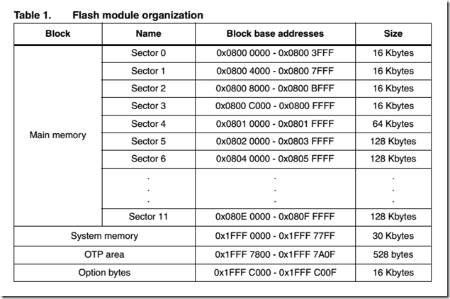
在STM32F4的编程手册上可找到FLASH的Sector划分,我们现在只操作Main memory:
参考Demo中的例子,将FLASH的页的其实地址(基地址)可定义如下:
/* Base address of the Flash sectors */ #define ADDR_FLASH_SECTOR_0 ((uint32_t)0x08000000) /* Base @ of Sector 0, 16 Kbytes */ #define ADDR_FLASH_SECTOR_1 ((uint32_t)0x08004000) /* Base @ of Sector 1, 16 Kbytes */ #define ADDR_FLASH_SECTOR_2 ((uint32_t)0x08008000) /* Base @ of Sector 2, 16 Kbytes */ #define ADDR_FLASH_SECTOR_3 ((uint32_t)0x0800C000) /* Base @ of Sector 3, 16 Kbytes */ #define ADDR_FLASH_SECTOR_4 ((uint32_t)0x08010000) /* Base @ of Sector 4, 64 Kbytes */ #define ADDR_FLASH_SECTOR_5 ((uint32_t)0x08020000) /* Base @ of Sector 5, 128 Kbytes */ #define ADDR_FLASH_SECTOR_6 ((uint32_t)0x08040000) /* Base @ of Sector 6, 128 Kbytes */ #define ADDR_FLASH_SECTOR_7 ((uint32_t)0x08060000) /* Base @ of Sector 7, 128 Kbytes */ #define ADDR_FLASH_SECTOR_8 ((uint32_t)0x08080000) /* Base @ of Sector 8, 128 Kbytes */ #define ADDR_FLASH_SECTOR_9 ((uint32_t)0x080A0000) /* Base @ of Sector 9, 128 Kbytes */ #define ADDR_FLASH_SECTOR_10 ((uint32_t)0x080C0000) /* Base @ of Sector 10, 128 Kbytes */ #define ADDR_FLASH_SECTOR_11 ((uint32_t)0x080E0000) /* Base @ of Sector 11, 128 Kbytes */
在库里边,FLASH的Sector编号定义如下,这是供库里边的几个函数使用的。需要将地址转换成Sector编号:
#define FLASH_Sector_0 ((uint16_t)0x0000) /*!< Sector Number 0 */ #define FLASH_Sector_1 ((uint16_t)0x0008) /*!< Sector Number 1 */ #define FLASH_Sector_2 ((uint16_t)0x0010) /*!< Sector Number 2 */ #define FLASH_Sector_3 ((uint16_t)0x0018) /*!< Sector Number 3 */ #define FLASH_Sector_4 ((uint16_t)0x0020) /*!< Sector Number 4 */ #define FLASH_Sector_5 ((uint16_t)0x0028) /*!< Sector Number 5 */ #define FLASH_Sector_6 ((uint16_t)0x0030) /*!< Sector Number 6 */ #define FLASH_Sector_7 ((uint16_t)0x0038) /*!< Sector Number 7 */ #define FLASH_Sector_8 ((uint16_t)0x0040) /*!< Sector Number 8 */ #define FLASH_Sector_9 ((uint16_t)0x0048) /*!< Sector Number 9 */ #define FLASH_Sector_10 ((uint16_t)0x0050) /*!< Sector Number 10 */ #define FLASH_Sector_11 ((uint16_t)0x0058) /*!< Sector Number 11 */
Demo中有将地址转换成Sector的代码:
uint32_t GetSector(uint32_t Address) { uint32_t sector = 0;
if((Address < ADDR_FLASH_SECTOR_1) && (Address >= ADDR_FLASH_SECTOR_0)) { sector = FLASH_Sector_0; } else if((Address < ADDR_FLASH_SECTOR_2) && (Address >= ADDR_FLASH_SECTOR_1)) { sector = FLASH_Sector_1; } else if((Address < ADDR_FLASH_SECTOR_3) && (Address >= ADDR_FLASH_SECTOR_2)) { sector = FLASH_Sector_2; } else if((Address < ADDR_FLASH_SECTOR_4) && (Address >= ADDR_FLASH_SECTOR_3)) { sector = FLASH_Sector_3; } else if((Address < ADDR_FLASH_SECTOR_5) && (Address >= ADDR_FLASH_SECTOR_4)) { sector = FLASH_Sector_4; } else if((Address < ADDR_FLASH_SECTOR_6) && (Address >= ADDR_FLASH_SECTOR_5)) { sector = FLASH_Sector_5; } else if((Address < ADDR_FLASH_SECTOR_7) && (Address >= ADDR_FLASH_SECTOR_6)) { sector = FLASH_Sector_6; } else if((Address < ADDR_FLASH_SECTOR_8) && (Address >= ADDR_FLASH_SECTOR_7)) { sector = FLASH_Sector_7; } else if((Address < ADDR_FLASH_SECTOR_9) && (Address >= ADDR_FLASH_SECTOR_8)) { sector = FLASH_Sector_8; } else if((Address < ADDR_FLASH_SECTOR_10) && (Address >= ADDR_FLASH_SECTOR_9)) { sector = FLASH_Sector_9; } else if((Address < ADDR_FLASH_SECTOR_11) && (Address >= ADDR_FLASH_SECTOR_10)) { sector = FLASH_Sector_10; } else/*(Address < FLASH_END_ADDR) && (Address >= ADDR_FLASH_SECTOR_11))*/ { sector = FLASH_Sector_11; }
return sector; }
有了这些定义之后,我们就可以开始正式操作FLASH了
首先,要向FLASH写入数据需要先将FLASH解锁。根据手册定义,解锁FLASH需要先向寄存器FLASH_KEYR写入0x45670123之后再向这个寄存器写入0xCDEF89AB。这两个数据在库中已经定义成了:FLASH_KEY1和FLASH_KEY2.
使用库函数不用这么麻烦,函数FLASH_Unlock()即可完成对FLASH的解锁。
解锁FLASH之后,使用函数FLASH_ClearFlag清除FLASH的状态寄存器。然后就可以对FLASH进行写操作了。我按照示例工程,擦除两块FLASH。
下边是操作FLASH的代码,首先擦除两块FLASH,然后向这两块FLASH中写入数据。最后进行校验:
要写入的数据定义:
#define DATA_32 ((uint32_t)0x12345678)
开始FLASH操作:
FLASH_Unlock(); //解锁FLASH后才能向FLASH中写数据。
//下面这个清flash的状态标志很重要,如果没有清可能会导致擦除flash失败或者不能擦除,我就遇到了这个问题,希望后面的兄弟一定要记得。 FLASH_ClearFlag(FLASH_FLAG_EOP | FLASH_FLAG_OPERR | FLASH_FLAG_WRPERR | FLASH_FLAG_PGAERR | FLASH_FLAG_PGPERR|FLASH_FLAG_PGSERR);
/* Get the number of the start and end sectors */ StartSector = GetSector(FLASH_USER_START_ADDR); //获取FLASH的Sector编号 EndSector = GetSector(FLASH_USER_END_ADDR);
//擦除FLASH for (i = StartSector; i < EndSector; i += 8) //每次FLASH编号增加8,可参考上边FLASH Sector的定义。 { /* Device voltage range supposed to be [2.7V to 3.6V], the operation will be done by word */ if (FLASH_EraseSector(i, VoltageRange_3) != FLASH_COMPLETE) { while (1) { } } }
/*擦除完毕*/ /*开始写入*/ Address = FLASH_USER_START_ADDR;
while (Address < FLASH_USER_END_ADDR) { if (FLASH_ProgramWord(Address, DATA_32) == FLASH_COMPLETE) //将DATA_32写入相应的地址。 { Address = Address + 4; } else { /* Error occurred while writing data in Flash memory. User can add here some code to deal with this error */ while (1) { } } }
FLASH_Lock(); //读FLASH不需要FLASH处于解锁状态。
//读出数据 检查写入值是否正确 Address = FLASH_USER_START_ADDR; MemoryProgramStatus = 0x0; while (Address < FLASH_USER_END_ADDR) { data32 = *(__IO uint32_t*)Address; //读FLASH中的数据,直接给出地址就行了。跟从内存中读数据一样。
if (data32 != DATA_32) { MemoryProgramStatus++; }
Address = Address + 4; }
下边是使用STLink Utility读出的数据,检查一下,确实写进去数据了:
参考文档是ST的 STM32F40xxx and STM32F41xxx Flash programming manual。可在ST网站下载。文档编号:PM0081。FLASH的有不少寄存器,各个含义手册上有详细介绍。我只是简单地看了下。使用库函数操作,好像不大需要详细理解这些寄存器了。 转载自:bobbat |
 微信公众号
微信公众号
 手机版
手机版


字节对齐有没有需要注意的地方